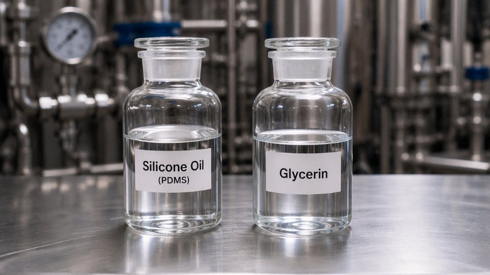
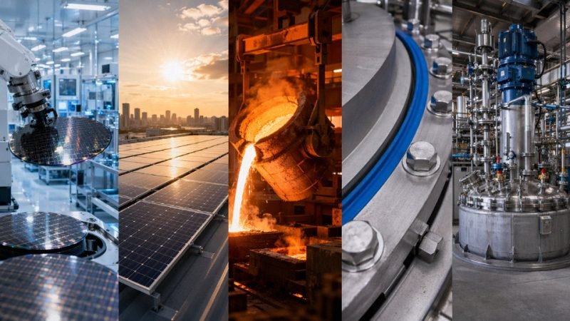
Silicon shows up everywhere in a modern facility — in the semiconductors controlling your drive systems, the gaskets sealing your high-temperature reactors, the solar panels on the warehouse roof — yet most procurement decisions treat it as a commodity line item until something fails. Specify the wrong silicone elastomer grade for a continuous 220 °C application and you’re looking at seal degradation within months, unplanned downtime, and a root-cause investigation that almost always traces back to a datasheet nobody read carefully. Get the purity spec wrong on a semiconductor substrate order and you’ve introduced defect densities that kill yield in ways that are genuinely hard to trace back to the incoming material.
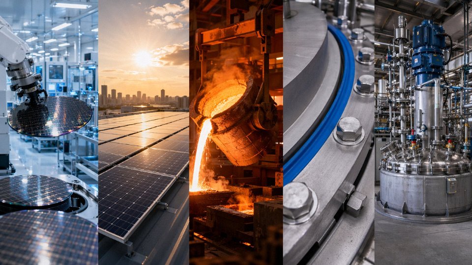
Silicon has five primary industrial uses: semiconductor and electronics manufacturing, silicone polymers and elastomers for sealing and thermal management, aluminum alloying to improve castability and strength, solar photovoltaic cell production, and specialty chemical synthesis. Each application draws on a different purity grade and processing route, ranging from 98–99% metallurgical-grade metal all the way to 99.9999999% (9N) electronic-grade crystal.
What makes this element worth understanding at a deeper level isn’t the chemistry — it’s the supply chain reality sitting behind it. Roughly 60–70% of the world’s silicon metal output, somewhere in the range of 3 million metric tons per year total, comes out of China, which means energy policy shifts, export controls, or even a bad hydropower season in Yunnan can move spot prices fast enough to matter on a quarterly budget. The five use cases aren’t equally exposed to that risk, and knowing which one you’re buying for changes how you should be sourcing it.
Use 1 — Semiconductor Fabrication: Silicon as the Backbone of Integrated Circuits
Getting silicon from quartzite rock to a finished 300 mm wafer ready for a lithography line is, honestly, one of the more remarkable industrial sequences in modern manufacturing — and it starts with a process that looks almost alarmingly low-tech for something producing 9N-purity material.
From Melt to Single-Crystal Ingot: The Czochralski Process
The Czochralski pull process begins with electronic-grade polysilicon loaded into a quartz crucible inside a vacuum-sealed furnace. The charge melts at 1,414°C. A small seed crystal — maybe 10 mm in diameter, precisely oriented along a specific crystallographic axis — is lowered until it just contacts the melt surface. Then the slow, controlled withdrawal begins: the seed is pulled upward and rotated simultaneously while the crucible rotates in the opposite direction. The combination of pull rate (typically 1–3 mm/min, depending on target diameter and dopant type) and rotation speed (roughly 5–20 RPM on each axis) determines the ingot’s diameter and crystalline perfection.
A finished ingot for leading-edge logic is 300 mm in diameter and can run 1–2 meters long. Wire sawing turns that into wafers approximately 775 µm thick — they’ll be ground and chemically-mechanically polished down further before any fab sees them. Kerf loss from wire sawing is real and it matters to procurement: you lose somewhere around 30–40% of the ingot mass to sawdust (called “kerf slurry”), which is why wafer costs track ingot yield so closely.
Doping: Where Electrical Behavior Gets Defined
A pure silicon wafer is, electrically speaking, not that useful on its own. The transistor switching behavior that makes CMOS logic work depends entirely on deliberate contamination — doping — at concentrations that sound almost impossibly small.
Phosphorus produces n-type silicon (extra electrons as carriers). Boron produces p-type (electron holes as carriers). The functional range spans roughly 10¹³ to 10¹⁸ atoms/cm³, and where you land in that range sets resistivity, carrier mobility, and ultimately how fast and efficiently a transistor switches. At 28 nm nodes, process engineers are working with well-characterized doping profiles. At 3 nm, the gate regions contain so few dopant atoms that statistical variation — just a handful of atoms more or fewer in one transistor versus its neighbor — starts to affect device behavior. That’s not a hypothetical; it’s why process control and wafer uniformity specs tighten dramatically at each node shrink.
Silicon retains dominance over GaAs and GaN in logic and memory chips despite their higher electron mobilityTrue
GaAs electron mobility (~8,500 cm²/V·s) and GaN exceed silicon (~1,400 cm²/V·s), but silicon's mature oxide (SiO₂) interface, established fab infrastructure, larger wafer diameters, and lower substrate cost make it economically and technically dominant for high-volume CMOS logic and DRAM/NAND production.
Industrial Scale and Why Competing Materials Haven’t Displaced Silicon
The global semiconductor silicon wafer market was valued at roughly USD 18 billion in 2023 — and that’s just the substrate before any fab processing begins. A single high-volume 300 mm fab can burn through more than 600,000 wafers per month. At that volume, substrate cost, yield, and supply chain reliability matter as much as raw material performance.
GaAs, SiC, and GaN all have electron mobility figures that silicon can’t match. SiC and GaN are increasingly dominant in power electronics and RF applications where those properties justify the price premium. But for logic and memory — the CMOS transistors in a CPU, the storage cells in NAND flash, the capacitors in DRAM — silicon’s thermally stable native oxide (SiO₂), its 200+ fabs worth of process infrastructure, and its scalability to 300 mm wafers keep it firmly in place. No competitor substrate currently offers that combination at volume.
In practice, “silicon vs. GaN” is rarely the right question for a logic or memory procurement team. The real decisions are around wafer grade, resistivity spec, and which Tier 1 suppliers can actually hold delivery commitments when the market tightens — which it does, cyclically and without much warning.
Use 2 — Solar Photovoltaic Cells: Converting Sunlight to Electricity at Terawatt Scale
Silicon’s 1.12 eV band gap isn’t just convenient for transistors — it happens to align almost perfectly with the peak photon flux of the solar spectrum, which is why the material dominates photovoltaics the same way it dominates logic chips. When a photon carrying energy above 1.12 eV strikes a silicon p-n junction, it excites an electron out of the valence band and leaves behind a positively charged hole. The built-in electric field at the junction — established during diffusion doping, typically phosphorus into a boron-doped p-type base — sweeps those carriers in opposite directions before they recombine. That charge separation produces a forward voltage of roughly 0.5–0.6 V per cell, depending on cell temperature, illumination intensity, and surface passivation quality. A single cell at that voltage is useless for grid applications, so manufacturers series-connect 60 or 72 cells per module (sometimes 96 for larger commercial formats), targeting module output in the 400–700 W range depending on cell efficiency and active area.
Monocrystalline, Polycrystalline, and Thin-Film: Why Mono-Si Won
Three silicon architectures have competed in the PV market for decades, and by 2024 monocrystalline silicon holds above 90% market share. That wasn’t inevitable — it was an economic and yield argument that played out over roughly fifteen years.
Monocrystalline silicon (mono-Si) cells, cut from Czochralski-pulled ingots, reach 22–26% commercial module efficiency. The exact figure depends on whether the cell uses PERC, TOPCon, or heterojunction (HJT) architecture, with HJT pushing toward the upper end. Polycrystalline silicon (poly-Si), cast in blocks and wire-sawn into wafers, lands at 17–20% — the grain boundaries scatter carriers and reduce minority carrier lifetime. Amorphous thin-film silicon (a-Si), deposited by plasma-enhanced CVD onto glass or flexible substrates, delivers only 6–10% efficiency, though its low deposition temperature and minimal silicon consumption kept it viable for building-integrated and portable applications.
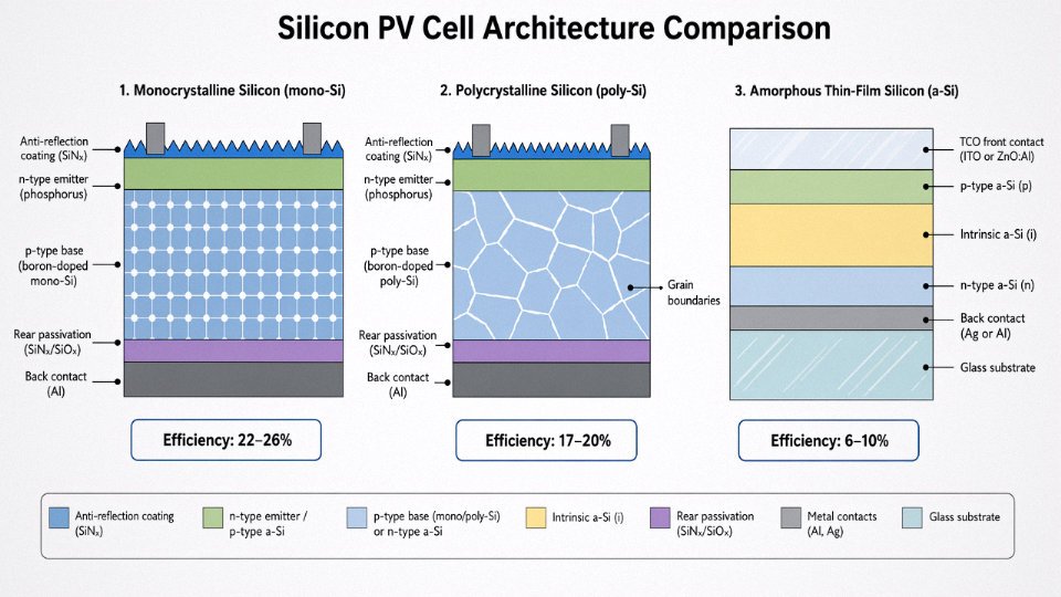
For most of the 2000s, poly-Si’s lower wafer cost offset its efficiency penalty; a factory could produce more watts per dollar from polycrystalline ingots than from Czochralski-pulled mono. The equation flipped when diamond-wire sawing cut mono-Si kerf losses enough to close the cost gap, and when PERC cell processing — essentially adding a rear passivation layer to reduce recombination — became standard on mono lines. Thin-film a-Si never fully recovered from that transition. In practice, if you’re procuring modules for a utility-scale project today, you’re almost certainly buying mono-Si PERC or TOPCon.
Polysilicon Supply Chain and the Terawatt Reality
Global installed solar PV capacity crossed 1.6 TW in 2024. Supplying that buildout requires several hundred thousand metric tons of solar-grade polysilicon annually — the exact figure depends on how aggressively wafer thickness is being reduced in any given year (the industry has gone from roughly 200 µm to 150 µm or below, meaningfully stretching each kilogram of polysilicon).
Polysilicon production routes both converge on trichlorosilane (SiHCl₃) decomposition. The Siemens CVD process deposits silicon onto thin carrier rods inside a bell-jar reactor — energy-intensive, batch-mode, but well-understood. Fluidized-bed reactor (FBR) routes feed SiHCl₃ over silicon seed particles continuously, consuming roughly 20–30% less electricity per kilogram, which matters enormously at scale. Both routes target solar-grade purity of 99.9999% (6N), comfortably below the 9N floor for semiconductor wafers but demanding enough that polysilicon capacity is a genuine supply-chain constraint during rapid PV deployment cycles.
Global installed solar PV capacity surpassed 1.6 TW in 2024True
Multiple energy agencies including IRENA and BloombergNEF tracked cumulative global solar PV installations crossing the 1.6 TW threshold during 2024, consistent with annual additions running at 350–400 GW in recent years.
End-of-Life Silicon: A Feedstock Problem Arriving Sooner Than Expected
Most silicon PV panels carry 25–30 year performance warranties, which means the first large commercial installations from the early 2000s are already reaching end of life. Panel volumes due for retirement will accelerate sharply through the 2030s. This is not a distant theoretical concern for procurement teams — pilot recovery facilities are operating now.
Mechanical delamination separates the encapsulant (usually EVA) from the glass and cell laminate, after which hydrofluoric acid etching removes the silicon nitride anti-reflection coating and metal contacts. Achieving 95%+ silicon reclaim by mass is technically feasible at the pilot scale; the harder problem is economic: recovered silicon currently needs reprocessing to re-enter the polysilicon supply chain, and the cost of that purification step versus virgin polysilicon is still unfavorable in most markets unless gate fees for panel disposal push the economics the other way. Expect this to change as landfill regulations tighten, particularly in the EU where the WEEE directive already covers PV modules.
Use 3 — Metallurgical Alloying and Steel Deoxidation: Silicon’s Largest Volume Application
People outside the metals industry are often surprised to learn that semiconductor wafers and solar cells — the applications that dominate headlines — account for a relatively small slice of global silicon consumption. The real volume goes into furnaces and ladles. Ferrosilicon production alone exceeds 9 million metric tons per year, and when you fold in aluminum-silicon casting alloys and direct silicon metal additions to steelmaking, metallurgical uses collectively consume somewhere in the range of 70–80% of world silicon metal output. The exact share shifts year to year depending on steel and automotive production cycles.
Deoxidation Chemistry in Steelmaking
When liquid steel comes off a basic oxygen furnace or electric arc furnace, dissolved oxygen levels typically run between 400 and 600 ppm. Leave that oxygen in and it causes porosity — gas pockets that form as the melt solidifies, leaving voids in castings and weak points in rolled bar or plate. Silicon fixes this problem fast and cheaply.
Additions of roughly 0.15–0.30 wt% silicon to the melt react preferentially with dissolved oxygen to form SiO₂ inclusions. Silicon has a much higher oxygen affinity than iron at steelmaking temperatures, so the reaction is thermodynamically decisive. The SiO₂ particles are lower density than steel and float toward the slag layer, dragging oxygen out of solution. Finished oxygen content after a proper silicon kill drops to below 20 ppm — sometimes well below 10 ppm depending on the grade target, ladle practice, and whether a combined Si/Al deoxidation scheme is used.
Getting the addition timing wrong matters. Add silicon too early in the tap, before slag carry-over is controlled, and you lose yield to reversion. Add it too late and the bath has already started cooling, reducing reaction kinetics. A melt shop running 150-tonne heats at a high pace will notice the difference in oxygen pick-up data pretty quickly if the deoxidation practice drifts.
Silicon additions during steelmaking reduce dissolved oxygen from 400–600 ppm down to below 20 ppm by forming SiO₂ slag inclusions that float to the surface.True
This deoxidation reaction is well-established in steelmaking metallurgy. Silicon's high oxygen affinity at molten steel temperatures makes it thermodynamically favorable; the resulting SiO₂ inclusions are less dense than liquid steel and rise into the slag layer, a mechanism documented across standard metallurgical references and confirmed by routine in-plant oxygen analysis.
Ferrosilicon Grades and Electrical Steel
Ferrosilicon is not a single product. The main commercial grades — FeSi45, FeSi65, FeSi75 — contain approximately 45, 65, and 75 wt% silicon respectively, the balance being iron with trace amounts of aluminum, calcium, and carbon depending on the source. FeSi75 is the workhorse grade for most steelmaking deoxidation and alloying work; FeSi45 and FeSi65 show up more often in foundry and cast iron applications where a lower silicon intensity is appropriate and cost per unit matters.
The higher-specification end of ferrosilicon use goes into electrical steel — sometimes called silicon steel — for transformer cores and electric motor stators. Silicon content in these grades runs 2–4 wt%, and the reason is purely electrical. Pure iron has an electrical resistivity of roughly 10 μΩ·cm. Push silicon to 3 wt% and that resistivity climbs toward 50 μΩ·cm, which cuts eddy current losses dramatically in laminated core stacks operating at 50 or 60 Hz. With EV motor production expanding rapidly, demand for higher-grade non-oriented electrical steel has been tightening the FeSi supply picture in ways that procurement teams started feeling around 2021–2022.
Aluminum-Silicon Casting Alloys
On the aluminum side, silicon’s role is different but equally fundamental. Al-Si casting alloys depend on silicon to make the melt actually castable. A380 — one of the most common die casting alloys in automotive use — carries 7.5–9.5 wt% Si. A413 pushes higher, to 11–13 wt% Si, and is used where maximum fluidity is needed for thin-walled or intricate die castings.
Silicon does several things simultaneously in these alloys. It depresses the melting point and widens the mushy zone in a way that gives good flow before solidification locks the casting. It reduces the thermal expansion coefficient, which matters for pistons running tight clearances inside a bore. And the hard silicon particles that precipitate during solidification provide wear resistance — critical in engine block cylinder bores, transmission housings, and piston skirts. Strontium or sodium modification of the eutectic silicon morphology (switching from coarse acicular to fine fibrous) can take a marginal mechanical property result and push it into spec without changing chemistry; most serious foundries run modified melts as a standard practice rather than optional.
Die casting A380 at a plant running ten-second cycle times on a 900-tonne press is unforgiving. If the Si content drifts below 7.5 wt% — which can happen if returns are poorly tracked — fluidity drops enough to cause misruns and cold shuts on thin ribs. If it creeps above 9.5 wt%, you start seeing hard spots that cause tool wear and dimensional issues in downstream machining. The chemistry window is real, and foundries that treat it casually pay for it in scrap rates.
Use 4 — Silicone Polymers: Engineering Chemistry from Medical Implants to Aerospace Sealants
Silicone is not silicon. That distinction matters more than it sounds. Walk into a procurement meeting where someone conflates the two and you’ll spend the first ten minutes untangling a materials mix-up that could have derailed a supplier qualification. Elemental silicon — the metallurgical or semiconductor-grade solid — is the upstream feedstock. Silicone polymers are a wholly different class of material: semi-inorganic, chain-structured, built around a Si-O backbone rather than a Si-Si crystal lattice, and engineered specifically for mechanical and chemical performance rather than electrical switching.
The Müller-Rochow Route: From Ore to Polymer Chain
The synthesis pathway is worth understanding because the economics of silicone pricing trace directly back to it. Metallurgical-grade silicon (roughly 98–99% pure, the same grade used in aluminum alloying, not the 9N wafer material) is milled to a fine powder and reacted with methyl chloride (CH₃Cl) in a fluidized-bed reactor at 250–350°C over a copper catalyst — occasionally with promoters like zinc or tin to shift the selectivity. This is the Müller-Rochow direct process, industrially standardized since the 1940s and still the dominant route.
The reactor output is a mixture of chlorosilanes, not a single compound. The key fraction is dimethyldichlorosilane (Me₂SiCl₂), which typically makes up 70–85% of the product mix depending on reactor conditions and catalyst age. The remaining chlorosilanes — trimethylchlorosilane, methyltrichlorosilane, and others — are separated by distillation and used to control chain-end capping and crosslink density downstream. Me₂SiCl₂ is then hydrolyzed with water, a reaction vigorous enough to require careful heat management, yielding silanediols that spontaneously condense to form the repeating [-Si(CH₃)₂-O-] unit. Chain length, and therefore viscosity and ultimate product form, is controlled by adjusting the ratio of monofunctional end-blockers to difunctional chain extenders.
Four Product Families, Each With Its Own Performance Logic
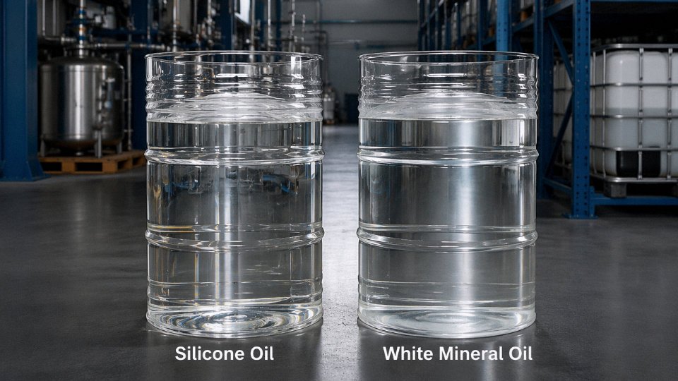
Silicone fluids cover an almost absurd viscosity range — from 0.65 cSt (thinner than water) up past 2,500,000 cSt for the highest-molecular-weight grades — and are used as transformer coolants, hydraulic media in sensitive actuators, mold-release agents, and heat-transfer fluids in pharmaceutical processes. The thermal stability across the -60°C to +230°C continuous service band (with short excursions tolerable to around 300°C, depending on the specific formulation and oxygen exposure) is genuinely hard to replicate with petroleum-based fluids.
Silicone elastomers and rubbers are where the biomedical and food-processing industries lean hardest. Shore A hardness typically runs 10–80, elongation at break can reach 700% in softer grades, and USP Class VI and ISO 10993 compliance opens the door to pacemaker lead insulation, long-dwell catheters, and breast implant shells. High-consistency rubber (HCR) is compression- or injection-molded; liquid silicone rubber (LSR) suits high-volume automated injection with cycle times under 30 seconds on a well-tuned press.
Silicone elastomers rated to USP Class VI are inherently biocompatible without any additives.False
USP Class VI and ISO 10993 biocompatibility depend on the complete compounded formulation — base polymer plus any fillers, pigments, cure-system residuals, and processing aids — not the PDMS backbone alone. Extractables and leachables testing is required for each specific formulation and end-use.
Silicone resins are crosslinked, ladder-structured materials rather than linear chains. They’re used as high-temperature dielectric coatings on motor windings and transformer components, rated to 250°C continuous service, and as binders in heat-resistant paints. They’re less flexible than elastomers but dimensionally stable under sustained thermal load.
RTV sealants and adhesives — both one-part (RTV-1, moisture-cure) and two-part (RTV-2, addition- or condensation-cure) systems — deliver elongation above 300% and realistic service lives exceeding 20 years in building curtain wall joints, which is why glazing engineers specified silicone for high-rise facades starting in the 1970s and never seriously revisited that decision. Getting the joint geometry right matters as much as the product selection; a sealant bead that’s too thin fails in fatigue regardless of the chemistry.
Aerospace and Defense: Where the Premium Is Non-Negotiable
In aerospace applications, silicone shows up in places most procurement managers never think about. Ablative thermal protection compounds on re-entry vehicles use silicone as the char-forming matrix — the controlled decomposition behavior under extreme heat flux is the actual design feature, not a flaw. On commercial aircraft interiors, silicone foam cavity fillers must meet FAR 25.853 flammability requirements, and the qualification process is long enough that substituting a “cheaper equivalent” mid-program is rarely a viable option. Conformal coatings on avionics PCBs are often silicone-based, qualified to MIL-I-46058C Type SR, because the combination of wide temperature cycling tolerance, moisture resistance, and reworkability with standard solvents suits a board that may need depot-level repair over a 30-year airframe life.
Regulatory Pressure and the Sustainability Picture
The EU REACH restriction on cyclic volatile methyl siloxanes — specifically D4 (octamethylcyclotetrasiloxane) and D5 (decamethylcyclopentasiloxane) — in rinse-off cosmetics at concentrations above 0.1% by weight has pushed formulators toward linear PDMS alternatives. This matters upstream because D4 and D5 are natural byproducts of the Müller-Rochow hydrolysis step, and managing their fate in the overall process affects both cost and regulatory compliance. In industrial silicone products — sealants, elastomers — the REACH restrictions do not currently apply in the same way, but regulatory trajectory suggests that will eventually tighten.
HCR scrap reclamation via pyrolysis is scaling at several compounders in Europe and Asia. The process recovers SiO₂ and methane as primary outputs; the recovered silica can re-enter the silicone filler supply chain, though purity specifications are still being standardized. It’s not a fully closed loop yet, but it’s a meaningful step away from landfill disposal of cured silicone waste, and some OEM customers are beginning to ask for it in their supply chain audits.
Use 5 — Glass, Optical Fibers, and Silica-Based Ceramics: [Silicon Dioxide](https://siliconchemicals.com/silica/) as a Structural and Photonic Material
Silicon dioxide — SiO₂ — is what most of the world actually handles when it handles “silicon” in everyday life, even if nobody calls it that. Float glass in a curtain wall, the fiber strand carrying a video call across an ocean, the lens inside a semiconductor lithography tool: all of them are engineered silica, and all depend on the same Si–O tetrahedral network chemistry that makes SiO₂ simultaneously transparent, thermally stubborn, and mechanically stiff.
The Float Glass Process: Liquid Tin as the World’s Flattest Surface
The Pilkington float process — developed in the late 1950s and now essentially universal for flat glass production — is one of the more elegant continuous manufacturing operations in existence. A batch of silica sand (~73 wt% SiO₂), soda ash, limestone, and minor additives is melted at roughly 1,500–1,600°C in a regenerative furnace, then poured onto a bath of molten tin held at around 1,000°C in an enclosed, slightly reducing atmosphere. The glass ribbon floats because its density (~2.5 g/cm³) is less than tin’s (~6.5 g/cm³). Gravity and surface tension do the leveling work. You can pull thicknesses from about 2 mm up to 25 mm in the same line by adjusting ribbon speed and width, and surface flatness deviations stay under roughly 0.1 mm across a 3-meter-wide ribbon — tolerances that would be essentially impossible to hit by grinding at volume. Virtually every pane of architectural glazing and automotive windshield glass on the planet comes off this kind of line.
Optical Fiber: 125 Micrometers Carrying 99% of Global Internet Traffic
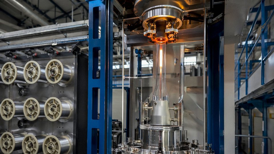
Optical fiber manufacturing starts with a preform — a fat cylinder of ultrapure fused silica built up through either modified chemical vapor deposition (MCVD) or outside vapor deposition (OVD). GeO₂ doping raises the core’s refractive index fractionally above the cladding; fluorine doping can lower the cladding index instead. Either way, the index differential confines light by total internal reflection. The preform is then drawn at around 2,000°C down to a 125 µm diameter fiber, thin enough that a strand 10 km long weighs next to nothing. Attenuation in a well-made single-mode fiber runs below 0.2 dB/km at 1,550 nm wavelength — meaning you can transmit a signal roughly 80–100 km before amplification, depending on the system design and splicing quality. That figure is why fiber dominates long-haul and subsea links. Coax or copper simply can’t touch it at distance.
Optical fiber carries approximately 99% of the world's long-distance internet trafficTrue
Undersea and terrestrial fiber optic cables form the primary physical backbone of global internet infrastructure; satellite links handle a small fraction of total bandwidth, and copper is largely confined to last-mile access connections.
Fused Silica in Semiconductor Lithography: Purity That Borders on Absurd
ArF excimer lasers used in deep-UV lithography emit at 193 nm — right at the edge of what silica can transmit without absorbing. The fused silica used for stepper lenses and windows has to be synthetic (not mineral quartz, which has too many inclusions), with hydroxyl (OH) content below about 1 ppm and birefringence held under 0.5 nm/cm. Why? Because any significant inhomogeneity scatters or polarizes the beam, blurring the feature printed on the wafer. A single lens element in an ArF immersion system might survive billions of laser pulses in service. That kind of radiation hardness doesn’t happen by accident — it requires precisely controlled OH doping during deposition and careful annealing schedules. This is not commodity glass.
Si₃N₄ and SiC Ceramics: When Metals Run Out of Temperature
Silicon nitride (Si₃N₄) and silicon carbide (SiC) are structural ceramics that happen to start from silicon chemistry, and they perform in environments where even superalloys struggle. Si₃N₄ sintered components can operate continuously at temperatures up to around 1,400°C with fracture toughness in the 6–8 MPa·m⁰·⁵ range — respectable for a ceramic, though you still design conservatively given the lack of plastic deformation before fracture. SiC ceramic matrix composites (CMC) have made it into commercial jet engine combustor liners, most visibly in the CFM LEAP family. The payoff is real: SiC CMC liners require substantially less cooling air than the nickel superalloy parts they replace — on the order of 40% less — which means that air can go toward combustion instead, improving thermal efficiency. Lower part weight is a secondary benefit, but the cooling air saving is what the thermodynamic argument rests on.
The practical catch with advanced ceramics is procurement and lead time. Si₃N₄ and SiC components from qualified suppliers often run 20–40 weeks out, and the machining and non-destructive inspection costs are steep enough that most applications justify them only when temperature, weight, or corrosion rules out metal entirely. For the right application, though — gas turbine hot sections, semiconductor process chamber components, high-temperature kiln furniture — there’s often no substitute.
How Silicon Is Produced: From Quartzite to Semiconductor-Grade Wafer Step by Step
The five application domains covered above — semiconductors, photovoltaics, alloys, silicones, and silica-based materials — all trace back to the same raw material: quartzite or high-purity quartz sand, essentially SiO2 dug out of the ground. What changes is how aggressively you purify it, and that’s where the cost and complexity live.
Carbothermic Reduction in the Electric Arc Furnace
Metallurgical-grade silicon starts in a submerged electric arc furnace running at somewhere between 1,800 and 2,000°C. The reaction is straightforward on paper:
SiO2 + 2C → Si + 2CO
In practice, the carbon charge is a blend of coal, petroleum coke, and woodchip — the woodchip isn’t just filler; it controls bed permeability so the CO can escape without building up pressure and causing eruptions. Get that blend wrong and you get bridging in the burden, which can cause a blowout and at minimum ruins a tap cycle. Batch sizes run roughly 10,000 to 40,000 kg depending on furnace rating, and energy consumption is typically 12–14 MWh per metric ton of silicon produced. That figure shifts depending on quartzite purity, electrode condition, and how well the furnace is sealed — a leaky furnace bleeds heat and pushes you toward the top of that range fast.
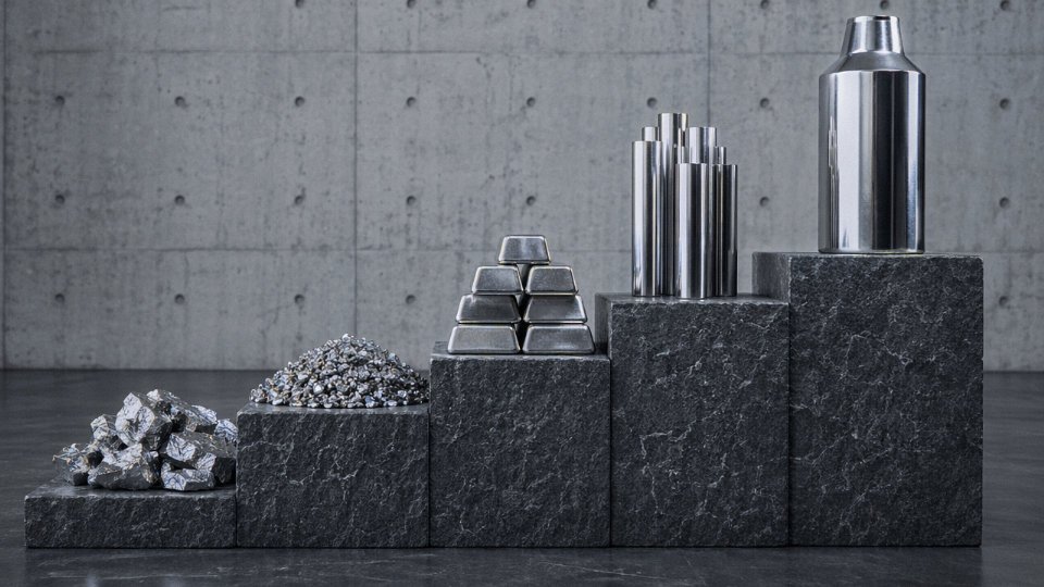
The output is MG-Si at 98–98.5% purity. Good enough for aluminum alloying and steelmaking. Nowhere near good enough for a transistor.
Siemens CVD: The Brutal Economics of Getting to 9N
To reach electronic grade, MG-Si is first reacted with anhydrous HCl to form trichlorosilane (SiHCl3). That intermediate is then fractionally distilled — repeatedly, in tall columns — to strip out boron, phosphorus, aluminum, and transition metals. Boron and phosphorus are the nasty ones; they’re dopants, so even a few parts per billion will shift the electrical behavior of finished wafers in ways that destroy device yield. Distillation removes them because their chloride compounds have different boiling points than SiHCl3, though getting that separation clean enough requires multiple passes.
The purified SiHCl3 then decomposes thermally inside a Siemens CVD reactor — a bell-jar vessel containing U-shaped silicon rods heated to around 1,100°C. Polysilicon deposits on the rods at 5–7 μm/min, building up over days into thick, high-purity cylinders. Power consumption here is 50–100 kWh/kg, which is why polysilicon cost tracks electricity prices so closely. Plants in regions with cheap hydropower have a genuine structural cost advantage; this isn’t theoretical.
Siemens CVD polysilicon production consumes significantly more energy per kilogram than the initial carbothermic reduction step.True
Carbothermic reduction runs roughly 12–14 MWh per metric ton (12–14 kWh/kg), while Siemens CVD deposition requires 50–100 kWh/kg of polysilicon — a 4x to 8x energy intensity increase driven by the high-temperature CVD process and the need to maintain precisely controlled reactor conditions over multi-day deposition runs.
Czochralski Growth: Turning Polysilicon into a Single Crystal
Polysilicon chunks get loaded into a quartz crucible, melted under argon atmosphere, and seeded with a small single-crystal silicon seed rod. The crystal is then pulled upward at 1–3 mm/min while rotating at 5–20 rpm — the rotation helps homogenize the melt temperature and controls dopant distribution across the ingot diameter. A typical Czochralski run yields a cylindrical ingot 1–2 meters long.
One detail that catches people off guard: oxygen from the quartz crucible dissolves into the melt and incorporates into the growing crystal at concentrations of roughly 10–18 ppma (per ASTM F121). This sounds like a contamination problem, and uncontrolled it is. But at the right concentration, those oxygen atoms precipitate during device thermal processing and act as internal gettering sites — they trap metallic impurities away from the active device layer. So oxygen content is deliberately targeted, not merely tolerated. Too low and you lose gettering effectiveness; too high and you get oxygen-induced stacking faults that kill yield.
Wafer Preparation: Where Geometry Becomes Spec
The ingot gets cropped at both ends, then sliced by multi-wire saws — each cut loses roughly 300 μm of kerf, which is pure material waste on what is by then very expensive silicon. After slicing, wafers go through lapping to flatten them, then etching to remove saw damage, then chemical-mechanical planarization (CMP) to achieve surface roughness Ra below 0.1 nm. That’s not a typo. Sub-angstrom roughness, measured across a 300 mm disk.
Leading-edge fabs specify total thickness variation (TTV) below 1 μm and site flatness (SFQR) below 25 nm across any given exposure site. Missing those specs means lithography tools can’t hold focus uniformly, and you start losing critical dimension control at the 3–5 nm node. For many device types, an epitaxial layer — 2–10 μm of lightly or heavily doped silicon — is deposited on the polished wafer surface before it ever enters a fab’s process flow.
The jump from 98% MG-Si to 99.9999999% wafer-ready silicon is, in terms of energy, cost, and process complexity, as large as any transformation in industrial manufacturing. That’s what the price differential reflects.
Comparing Silicon’s Five Industrial Roles: Performance, Volume, and Value Side by Side
The five applications covered in this article are not competing uses — they draw on almost entirely separate supply chains, different refining stages, and wildly different economics. A procurement manager sourcing ferrosilicon for a steel mill and one sourcing electronic-grade wafers are, in practical terms, operating in different industries that happen to share a feedstock mineral. The table below makes the contrast concrete.
Reference Comparison Across All Five Domains
| Use Case | Annual Silicon Consumption | Required Purity | Approx. Input Silicon Value | Est. CAGR 2024–2030 | Primary Risk Factor |
|---|---|---|---|---|---|
| Metallurgical / FeSi alloys | ~2.0 Mt | 98–98.5% (MG-Si) | USD 1.2–1.8/kg | 2–4% | Energy cost volatility; China export policy |
| Solar polysilicon | ~550,000–650,000 t | 99.9999% (6N) | USD 6–10/kg | 8–12% | Oversupply cycles; geopolitical sourcing risk |
| Semiconductor wafers | ~80,000–100,000 t | 99.9999999% (9N) | USD 80–150/kg (silicon content equiv.) | 6–9% | Fab yield losses; EUV tooling lead times |
| Silicone polymers | ~850,000–950,000 t Si equiv. | ~99% (technical-grade) | USD 3–5/kg | 4–7% | Chloromethane supply; regulatory pressure on VOC emissions |
| Glass / optical fiber / ceramics | ~450,000–550,000 t SiO₂ equiv. | Variable: float glass to 99.99% fused silica | USD 0.05–2/kg depending on form | 3–5% | Specialty silica supply; preform manufacturing capacity |
Consumption figures are approximate and shift with economic cycles. Solar polysilicon in particular swung dramatically between 2021 and 2024 — prices hit USD 30+/kg at the 2022 peak before corrective capacity expansions drove them back toward the lower end of the range above.
The Purity-Cost Curve Is Exponential, Not Linear
This is the single most important relationship to internalize if you’re making capital allocation or procurement decisions across silicon supply chains. Moving from metallurgical-grade silicon at roughly USD 1–2/kg to solar-grade polysilicon at USD 6–10/kg sounds like a modest step — six times the price. But the actual processing cost per kilogram roughly multiplies by 20–40x when you account for the Siemens reactor economics, energy consumption, and yield losses involved in the chemical vapor deposition refining cycle. Then the jump from 6N solar-grade to 9N semiconductor-grade is another order of magnitude beyond that, because you are now dealing with Czochralski crystal pulling under stringent atmospheric control, precision slicing with diamond wire saws losing 15–25% of the boule as kerf, epitaxial deposition, and a qualification trail that can stretch 12–18 months at a new fab.
Semiconductor-grade silicon requires a purity of 99.9999999% (nine nines), achieved through Czochralski or float-zone crystal growthTrue
This 9N specification is an industry-standard requirement for leading-edge logic and memory wafer production. At impurity levels above roughly 1 part per billion, carrier mobility and junction leakage behavior degrade in ways that compromise transistor switching characteristics at sub-10 nm nodes.
Supply Chain Concentration Is the Cross-Cutting Risk
China’s share of global metallurgical silicon production sits around 60–70% depending on the year, and its share of polysilicon is even higher — closer to 80–85% of nameplate capacity as of the mid-2020s. For ferrosilicon the figure is roughly 65%. That kind of concentration is tolerable when trade relationships are stable, but plant managers who lived through the 2021 magnesium shortage — when a Chinese power-rationing episode took out a disproportionate fraction of global supply in weeks — have a visceral sense of what that dependency actually means for a production line.
The US CHIPS Act and the EU Critical Raw Materials Act both name silicon as a strategic material, and that designation is starting to generate real capital flows. Wacker Chemie in Germany, REC Silicon restarting capacity in the United States, and Polymatech’s announced polysilicon project in India are examples of the geographic diversification effort underway. Whether those projects alter the fundamental concentration picture meaningfully by 2030 is genuinely uncertain — Wacker and REC together represent a small fraction of Chinese nameplate capacity, and polysilicon plants take 3–5 years to build and qualify before they ship product into leading-edge supply chains. In practice, the diversification is real but partial, and procurement teams sourcing solar or semiconductor polysilicon should be modeling dual-source scenarios rather than assuming a new equilibrium by the end of the decade.
The metallurgical segment, by contrast, is more geographically distributed and price-elastic. The glass and ceramics segment operates on SiO₂ feedstocks sourced more locally in most regions. The risk profile genuinely differs across the five domains — which is why treating “silicon supply risk” as a single variable in a risk register is a mistake.
Emerging and Next-Generation Silicon Applications on the Industrial Horizon
The five uses covered above account for the vast majority of silicon consumed today. But the material’s roadmap over the next decade is, frankly, more interesting than anything already commercialized — and procurement engineers and plant managers who ignore it will be caught flat-footed when supply chains shift.
Silicon Anode Batteries: Chasing Capacity Against a Mechanical Problem
Silicon’s theoretical specific capacity of 3,579 mAh/g versus graphite’s 372 mAh/g sounds like a solved argument. It isn’t. The problem is mechanical: silicon swells roughly 300% by volume during lithiation, and that expansion fractures particles, ruptures the solid-electrolyte interphase layer, and drives rapid capacity fade. A cell that looks promising at cycle 50 can be unusable by cycle 300. Anyone who has worked with early pouch cells using high-silicon anodes has seen this firsthand — the cells physically deform.
The current commercial answer is a compromise: nano-silicon composite anodes blended with graphite at roughly 5–15 wt% silicon, which buffers expansion enough to survive real-world cycle life requirements. Cells built on this architecture deliver somewhere in the 280–320 Wh/kg range at the cell level, depending heavily on cathode chemistry and cell format, compared to 240–260 Wh/kg for graphite-only designs. That gap is meaningful in EV applications where pack weight directly affects range. Sila Nanotechnologies, Enovix, and Panasonic are among the groups pushing toward higher silicon content — targeting above 500 Wh/kg by around 2028 — using approaches that range from silicon-dominant anodes with engineered void space to fully three-dimensional cell architectures that tolerate expansion geometrically rather than fighting it chemically.
Silicon's theoretical anode capacity of 3,579 mAh/g is roughly 9.6 times that of conventional graphite at 372 mAh/gTrue
These are well-established electrochemical values based on the Li15Si4 alloying reaction for silicon and LiC6 intercalation for graphite, widely reported in peer-reviewed electrochemistry literature
Whether the 500 Wh/kg targets hold to schedule is genuinely uncertain. SEI re-formation consumes lithium inventory irreversibly, and scaling nano-silicon synthesis cost-effectively at tonnage quantities is still an unsolved manufacturing problem, not just a chemistry one.
Silicon Photonics: Moving Data at the Speed of Light, on a Wafer
Single-crystal silicon is a surprisingly capable optical waveguide when you structure it correctly. Silicon-on-insulator platforms — typically 220 nm of device silicon sitting above a 2 μm buried oxide layer — confine 1,310 nm and 1,550 nm telecom wavelengths effectively, with propagation losses below about 2 dB/cm in well-fabricated waveguides. That figure depends on sidewall roughness from the etch process; a sloppy etch easily doubles the loss.
Intel, GlobalFoundries, and TSMC now offer silicon photonics process design kits through multi-project wafer shuttles, which has dramatically lowered the barrier for integrating optical transceivers directly with CMOS logic. Data centers running 400G and 800G interconnects are the primary driver. Transceiver shipments in silicon photonics are projected to exceed 10 million units annually by the mid-2020s. For a procurement engineer sourcing optical interconnect components today, this technology is no longer experimental — it is a current procurement decision, not a future one.
Silicon Quantum Computing: The Slow Horse That Might Win
Superconducting qubits get the press coverage, but the silicon spin-qubit approach has one advantage that matters enormously at scale: it is inherently CMOS-compatible. Phosphorus donor atoms implanted into isotopically purified silicon-28 — chosen because ²⁸Si has zero nuclear spin, eliminating a major decoherence source — achieve qubit coherence times exceeding 30 seconds at millikelvin temperatures. That is orders of magnitude longer than superconducting qubit coherence times, which typically run in the microsecond-to-millisecond range.
Groups at UNSW Sydney, QuTech in the Netherlands, and Intel (whose Horse Ridge cryogenic control chip is itself a silicon product) have demonstrated two-qubit gate fidelities above 99.5%. Fault-tolerant quantum computing likely requires gate fidelities above 99.9%, so there is real work remaining. But the pathway from laboratory spin-qubit demonstrations to a manufacturable quantum processor that can be fabbed on existing silicon infrastructure is more credible for silicon than for any competing platform.
Whether this translates into a procurement or supply-chain event before 2030 is debatable. Isotopically enriched ²⁸Si feedstock is already a specialty chemical market, small-volume and high-cost, supplied by a handful of producers. If silicon quantum computing scales, that supply chain will need to grow from grams to kilograms — and that transition rarely happens smoothly.
Frequently Asked Questions About Silicon Uses
What is the single largest use of silicon by volume?
Metallurgical applications — ferrosilicon for steelmaking deoxidation plus aluminum-silicon casting alloys — consume well over 70% of global silicon metal output by weight. That figure surprises a lot of people who assume semiconductors or solar panels dominate. They don’t, not even close. A single mid-sized steel mill running continuous casting can go through more silicon in a month than a wafer fab uses in a year. The semiconductor and solar industries get the press, but the tonnage belongs to metallurgy. Global silicon metal production runs roughly 3 million metric tons per year (the exact figure shifts with Chinese smelter output, energy costs, and downstream steel demand), and the vast majority of that never gets anywhere near a cleanroom.
Is silicon the same as silicone?
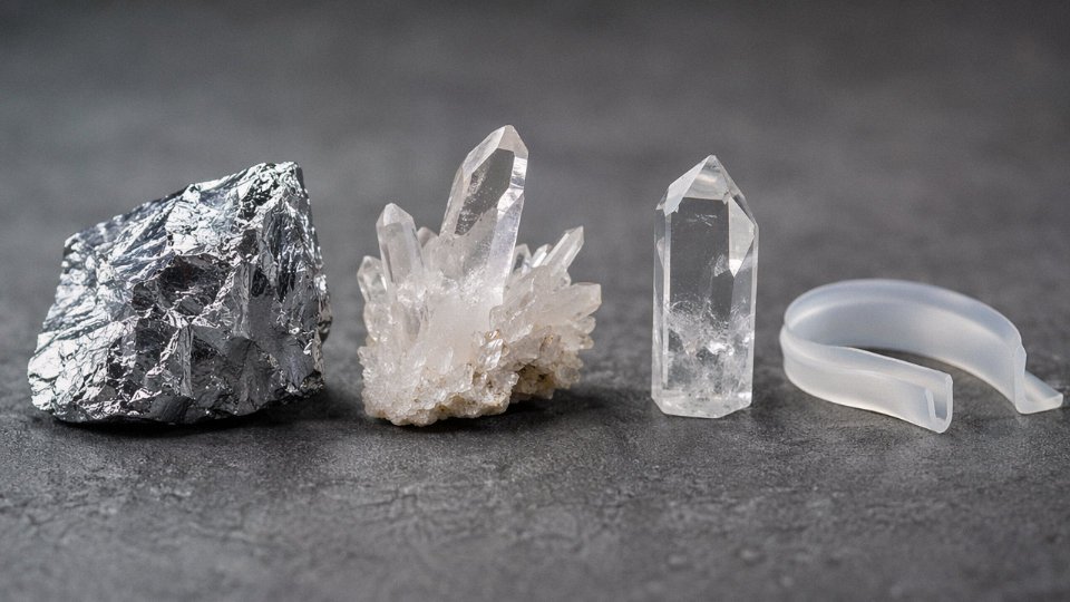
No, and the confusion causes real procurement errors. Silicon (Si) is a solid crystalline or metallurgical element — what you have when you reduce quartzite in an electric arc furnace or grow a single-crystal boule in a Czochralski puller. Silicone is a synthetic polymer built around a Si-O backbone with organic side groups, typically methyl or phenyl, hanging off it. Getting from elemental silicon to silicone requires reacting silicon metal with methyl chloride over a copper catalyst to produce chlorosilanes, then hydrolyzing and polymerizing those intermediates — a multi-step industrial chemistry route that happens at dedicated silicone chemical plants, not at a metallurgical smelter.
They share the element silicon, but physically and chemically they have almost nothing in common. Elemental silicon is a hard, brittle semiconductor. Silicone elastomers are flexible, chemically inert, and service-rated from roughly -60°C to +230°C continuously. Ordering the wrong one for a gasket application or a wafer-cleaning fluid isn’t a minor mistake.
Silicone and silicon are the same materialFalse
Silicon is an elemental solid (Si); silicone is a Si-O backbone polymer synthesized from silicon via chlorosilane intermediates. They are chemically and physically distinct materials with entirely different industrial supply chains.
Why does silicon dominate computer chips when other semiconductors exist?
The short answer is that no other material bundles everything silicon offers at comparable cost. The 1.12 eV band gap is workable for room-temperature logic. The native oxide — SiO2 — forms thermally at 900–1100°C with a dielectric strength around 9 MV/cm, which gave the industry a built-in gate insulator that gallium arsenide simply cannot match. Add abundant raw material, well-characterized phosphorus and boron doping chemistry, and fifty-plus years of accumulated process infrastructure, and you have a moat that compound semiconductors keep running into. Gallium nitride and silicon carbide are genuinely superior for power electronics and RF. But for high-volume digital logic? Silicon’s economics are brutal to compete against.
How pure does silicon need to be for solar panels?
Solar-grade polysilicon sits at roughly 99.9999% purity — 6N in shorthand. That means metallic impurities like boron and phosphorus need to be below about 1 part per billion atomic each. Those elements aren’t just contaminants; at even trace concentrations they create recombination centers that shorten minority carrier lifetime and drag down cell efficiency in ways that show up directly on your watts-per-panel output. Semiconductor-grade silicon pushes to 9N (99.9999999%), which is meaningfully harder to achieve and commands a correspondingly higher price. The gap between 6N and 9N isn’t trivial — it represents a completely different purification regime.
Can silicon be recycled from end-of-life solar panels?
Yes, and the industry is finally taking it seriously. Thermal, chemical (typically HF/HNO₃ etching sequences), and mechanical delamination processes can recover somewhere between 85–95% of the silicon from expired modules, depending on cell architecture and how well the encapsulant separates. Recovered material is currently being evaluated as metallurgical-grade feedstock and, in some pilot programs, as a route back toward solar-grade recycled polysilicon. This matters because the carbon intensity of virgin Siemens-process polysilicon is substantial — closing that loop would meaningfully change the lifecycle emissions profile of PV manufacturing. It’s still emerging at industrial scale, and purity consistency of recycled feedstock remains a real technical challenge, but the economics are tightening as first-generation utility-scale installations start hitting end-of-life in volume.
What is the difference between silicon and silica?
Silica (SiO₂) is the oxidized form — quartz, sand, flint. It’s everywhere and in its raw form costs almost nothing. Elemental silicon (Si) is what you get when you reduce silica with carbon in an electric arc furnace at roughly 1,500–2,000°C: you’re stripping oxygen away to liberate the silicon. Silica itself goes directly into glass, ceramics, concrete filler, and optical fiber preforms without ever becoming elemental silicon. Elemental silicon is what the semiconductor, solar, and metallurgical industries actually need. Same underlying element, completely different material, completely different supply chain, and a price difference of several orders of magnitude per kilogram once you get to semiconductor-grade.