Adhesion failure in electronic assemblies rarely announces itself early. A printed circuit board laminate that delaminated under thermal cycling, an encapsulant that lifted from a semiconductor die after 500 hours of humidity exposure, a coated architectural glass panel that lost its functional layer within two seasons — these are not design flaws in isolation. They are the predictable outcome of inadequate interfacial chemistry between inorganic substrates and organic polymer systems. The rework costs alone can run into the tens of thousands of dollars per production lot, and in semiconductor packaging, a single yield excursion traced to poor die-attach adhesion can halt a line for days.
Silane coupling agents are bifunctional organosilicon molecules that bond chemically to both inorganic surfaces — glass, silica, metals, and semiconductor oxides — and organic polymer matrices. Applied at concentrations typically ranging from 0.1% to 2% by weight depending on substrate, formulation type, and process method, they increase interfacial adhesion strength by 200–400% over untreated surfaces, dramatically reducing delamination, moisture ingress, and long-term reliability failures across electronics, semiconductor packaging, and glass treatment.
What makes the chemistry genuinely interesting is how a molecule that weighs less than 300 g/mol can determine whether a $40 semiconductor package survives ten years in an automotive engine bay or fails its first thermal shock test. Aminosilanes, epoxysilanes, and their variants each solve a different piece of that problem — and choosing the wrong one, or applying the right one incorrectly, produces failures that are expensive and often misattributed until it is far too late.
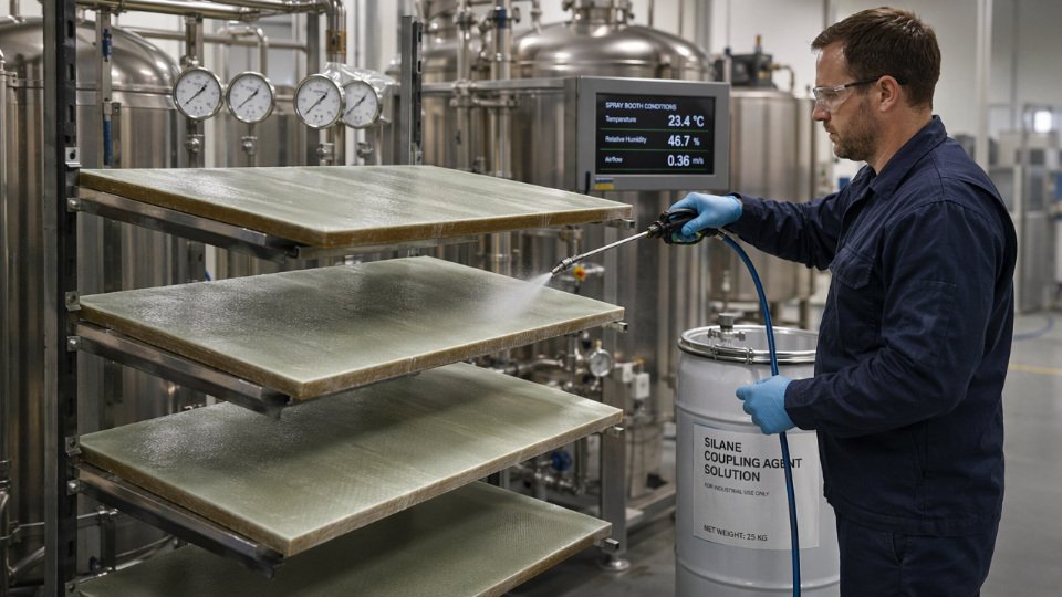
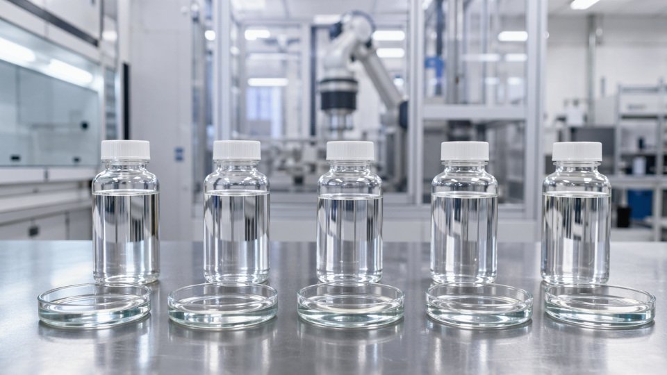
 being applied to glass fiber rovings in an industrial electronics materials production facility](https://siliconchemicals.com/wp-content/uploads/2026/06/silane-coupling-agent-electronics-semiconductors-glass-01-hero.jpg)
Printed Circuit Board Fabrication: Silane Treatment of Glass Fiber and Copper Foil
Glass fiber reinforced laminates — FR-4, Rogers hydrocarbon ceramic, and PTFE-based substrates — represent the single largest volume application of silane coupling agents in electronics. The reason is structural: E-glass fiber surfaces carry a high density of silanol groups (Si–OH) left over from the fiber drawing process, and these groups react readily with the alkoxy groups of a silane coupling agent to form stable covalent Si–O–Si bonds. Without that chemical bridge, the epoxy or PTFE matrix has no durable attachment to the fiber surface and relies only on mechanical interlocking and weak van der Waals forces. Under thermal cycling, moisture ingress, or drilling stress, untreated interfaces fail first.
Glass Fiber Sizing: Where the Chemistry Happens
The silane is applied inline, immediately after the fiber is drawn from the bushing, while the surface is still chemically reactive. A sizing bath typically contains silane dissolved at 0.1–2.0 wt% in deionized water or a water-isopropanol blend, adjusted to pH 3.5–5.5 to catalyze hydrolysis without premature oligomerization. Individual filaments pass through the bath, pick up a nanometer-scale silane film, and are then dried at 110–150 °C before being gathered into rovings or woven into fabric.
The performance payoff is measurable. Interlaminar shear strength (ILSS) on silane-treated glass/epoxy composites typically improves 200–400% over untreated controls — the actual uplift depends on fiber surface area, silane concentration, cure temperature, and resin stoichiometry. Moisture resistance also improves substantially; treated laminates show 30–60% lower water absorption after 24-hour boil tests, which directly reduces blister risk during lead-free reflow soldering at 260 °C.
Matching Silane Chemistry to Resin System
Silane selection is not interchangeable across resin systems. Using the wrong coupling agent can actually reduce adhesion by blocking reactive surface sites without forming a compatible bond with the matrix.
For standard FR-4 epoxy laminates, aminosilanes — primarily APTES (3-aminopropyltriethoxysilane) and APDMES (3-aminopropylmethyldiethoxysilane) — are the dominant choice. The terminal amine group reacts directly with epoxide rings during laminate cure, integrating the silane into the crosslinked network rather than leaving it as a weak boundary layer.
Methacryloxy silanes, particularly MPS (3-methacryloxypropyltrimethoxysilane), are used with vinyl ester and unsaturated polyester systems where free-radical crosslinking is the cure mechanism. The methacrylate end group copolymerizes into the resin network during cure.
PTFE-based and hydrocarbon ceramic substrates for high-frequency applications are the difficult case. PTFE is chemically inert, so conventional aminosilane or epoxysilane chemistry provides minimal benefit on the resin side. Specialized fluoroalkylsilanes improve wettability and mechanical keying at the fiber–PTFE interface, though this remains an area where formulation know-how matters more than off-the-shelf product selection.
| Silane Type | Compatible Resin System | Key Performance Metric | Typical Processing Temperature |
|---|---|---|---|
| Aminosilane (APTES, APDMES) | Epoxy (FR-4, halogen-free) | ILSS +200–400%; peel strength +40–80% | 150–180 °C laminate cure |
| Methacryloxy silane (MPS) | Vinyl ester, unsaturated polyester | Flexural strength +30–60% | 120–160 °C cure |
| Epoxysilane (GPS) | Epoxy, phenolic | Adhesion in humid aging +50–70% | 160–175 °C |
| Fluoroalkylsilane | PTFE, hydrocarbon ceramic | Surface energy reduction; interface wetting | 200–260 °C sintering range |
Copper Foil Treatment and Signal Integrity
Copper foil in multilayer PCBs receives a separate silane treatment step before lamination. An aminosilane or epoxysilane solution is applied to the copper surface — either by roll coating or spray — to build a molecular adhesion layer between the copper and the prepreg resin. In fine-line HDI boards with trace widths below 50 µm, peel strength at the copper–dielectric interface is a reliability-critical parameter. Delamination at this interface under thermal stress creates micro-cracks that disrupt impedance continuity and generate signal integrity failures at high data rates.
There is an electrical performance dimension that procurement teams sometimes underweight. At frequencies above 10 GHz — relevant for 5G mmWave boards and high-speed server interconnects — even trace ionic contamination from silane synthesis byproducts or improperly hydrolyzed oligomers can measurably increase the dissipation factor (Df). For Rogers or Megtron-class laminate production, specifying low-ionic-residue, high-purity silanes with consistent hydrolysis behavior is not optional.
Using an incorrectly matched silane coupling agent on PTFE-based high-frequency substrates provides no meaningful adhesion improvement over untreated fiberTrue
PTFE lacks reactive surface groups that form covalent bonds with standard aminosilane or epoxysilane organofunctional groups; without surface fluorination or plasma pre-treatment, standard silanes cannot chemically anchor to the PTFE matrix phase, leaving only weak physisorption
Operational warning: Silane bath concentration and pH must be monitored continuously in production. Hydrolysis is fast at low pH but oligomerization accelerates above pH 6, depositing thick, poorly bonded silane aggregates on fiber surfaces that actually reduce ILSS. A bath with drifted pH above 6.5 can turn a performance gain into a delamination risk — and the failure often doesn’t appear until thermal cycling during board assembly, not during incoming laminate inspection.
Semiconductor Packaging: Die Attach, Underfill, and Molding Compound Adhesion
The reliability problem in semiconductor packaging is fundamentally a mechanics problem dressed up as a chemistry problem. Every time a packaged device cycles from –55°C to +150°C during JEDEC JESD22-A104 qualification, the silicon die expands at roughly 2.6 ppm/°C while the copper substrate beneath it moves at 17 ppm/°C. The epoxy mold compound sits somewhere between 8 and 15 ppm/°C depending on filler loading and resin system. Those three mismatched layers are bonded at interfaces that, without proper adhesion promotion, will begin to delaminate after as few as a few hundred thermal cycles. In flip-chip BGA and advanced 3D stacked packages, where die-to-substrate standoff heights are measured in tens of microns, even a partial delamination front at the underfill-to-substrate interface creates a moisture ingress path that accelerates corrosion and ultimately kills the device in the field.
Silane coupling agents address this problem at two distinct points in the packaging process: as additives inside the formulation, and as a surface pre-treatment applied before dispensing.
Silane as a Formulation Additive in EMC and Underfill
Epoxy molding compounds typically contain 70–85 wt% inorganic filler — predominantly fused silica, with alumina added in thermally demanding packages. Without surface treatment, the interface between each filler particle and the surrounding epoxy matrix is the weakest link in the system. Epoxysilanes such as 3-glycidoxypropyltrimethoxysilane (GPS, commonly called KH-560 or A-187) and aminosilanes such as 3-aminopropyltriethoxysilane (APTES, A-1100) are incorporated at 0.2–1.5 wt% relative to filler weight — the right loading depends on filler surface area, particle size distribution, and the resin’s amine or anhydride cure system. During high-temperature compounding and cure, the silane hydrolyzes and condenses onto the silica surface while its organofunctional end reacts into the epoxy network. The result is a covalently bonded filler-matrix interface that dramatically reduces stress concentration at the particle level.
Aminosilanes and epoxysilanes together account for roughly 45–55% of all silane coupling agent consumption across electronics and semiconductor packaging, which reflects just how critical this filler-coupling role has become as package designs push filler loadings higher to manage CTE and thermal conductivity simultaneously.
Surface Pre-Treatment of Substrates and Die
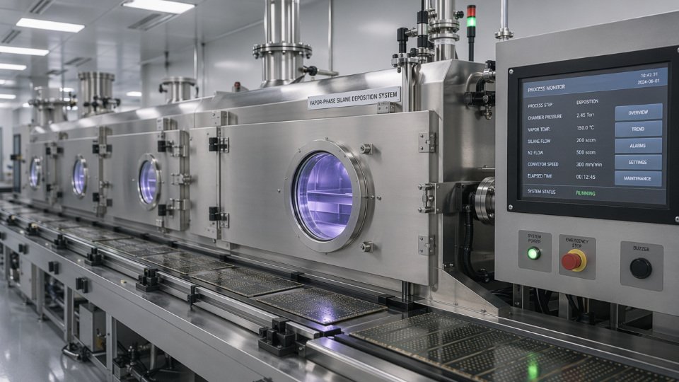
For high-volume advanced packaging lines, vapor-phase silane deposition has largely replaced wet-bath pre-treatment of lead frames, organic substrates, and die surfaces. The reason is control. A desiccator-style vapor chamber or an inline tunnel system deposits a self-limiting monolayer — typically 1–5 nm thick — without the liquid-handling variables of bath concentration drift, drag-out contamination, or drying uniformity. A production line running several thousand substrate strips per shift cannot afford the process variation that comes from a bath whose silane concentration drifts by 15% across a working day. Vapor deposition eliminates that variable and is compatible with automated inline handling.
Moisture Sensitivity Level and Reliability Payoff
The practical output of well-executed silane treatment is measurable in MSL testing. Packages built with silane-optimized underfill formulations — and pre-treated substrates — can reduce delamination incidence during 85°C/85% relative humidity preconditioning (JEDEC MSL testing) by 60–80% compared to untreated controls. That difference frequently translates to qualifying at MSL 1 rather than MSL 3, which means the device can sit on a moisture-sensitive device floor for unlimited time rather than being confined to a dry bag with a 168-hour clock. For customers assembling products with long production queues, that is a genuine manufacturing yield and logistics benefit, not a marginal one.
Silane-containing underfill formulations can reduce delamination rates in JEDEC MSL preconditioning by 60–80% compared to untreated controls.True
This range is reported in formulation studies comparing silane-modified and unmodified epoxy underfills under standardized 85°C/85% RH preconditioning protocols; the actual improvement depends on silane type, loading, filler surface area, and cure conditions.
Specialty Packages and Sulfur-Functional Silanes
Bis-silanes — specifically bis[3-(triethoxysilyl)propyl]tetrasulfide (TESPT) and bis[3-(triethoxysilyl)propyl]disulfide (TESPD) — appear in certain specialty packaging formulations where enhanced moisture barrier performance is the design target rather than pure adhesion strength. Their sulfur bridges provide additional crosslink density and flexibility, which matters in packages with unusual geometries or those expected to operate in high-humidity environments without hermetic sealing.
Purity Requirements at Wafer Level
One operational boundary worth stating plainly: the purity grade of silane used in any process that touches a gate dielectric or active device surface is non-negotiable. Front-end wafer-level processes require silanes with total metal content below 1 ppm and chloride below 10 ppm. Ionic contamination at those interfaces shifts threshold voltages and degrades gate oxide integrity in ways that don’t always show up immediately in electrical test but will surface as early field failures. Using a packaging-grade silane in a wafer-level application to reduce material cost is the kind of decision that generates an expensive customer return investigation six months after shipment.
Wafer-Level Dielectric and Photoresist Adhesion Promotion in Semiconductor Fabrication
Front-end wafer processing sits at the opposite end of the silane consumption curve from packaging — volumes are tiny, but purity requirements and cost sensitivity per wafer are extreme. Getting adhesion promotion wrong at this stage means lithographic defects, resist lift-off, or pattern collapse. Any of those outcomes scraps a wafer that may already carry dozens of process steps worth of value.
HMDS as the Workhorse Adhesion Promoter
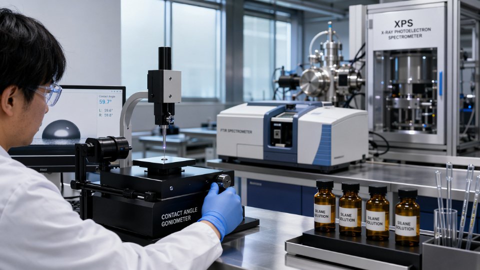
Hexamethyldisilazane (HMDS, CAS 999-97-3) has dominated photoresist adhesion promotion on silicon dioxide and silicon nitride surfaces for decades, and the reason is straightforward chemistry. Freshly cleaned or UV-ozone-treated wafer surfaces carry dense populations of silanol groups (Si–OH). These groups are hydrophilic; water vapor adsorbs readily, and conventional novolac or chemically amplified resists spread unevenly and delaminate during developer immersion if silanols are left intact. HMDS reacts with paired surface silanols to release ammonia (NH₃) and deposit trimethylsilyl (–Si(CH₃)₃) groups in their place. The resulting surface switches from hydrophilic to hydrophobic — measured water contact angles typically shift from below 10° to 60–80°, depending on surface oxide quality and process completeness.
HMDS vapor phase treatment converts hydrophilic silanol-rich wafer surfaces to hydrophobic trimethylsilyl-terminated surfaces, improving photoresist adhesion and reducing defect density in photolithography.True
The reaction of HMDS with surface silanols to form trimethylsilyl groups and release ammonia is well-established surface chemistry, documented in semiconductor process literature and equipment vendor process guides for decades.
The Vapor Prime Process: Why Liquid Application Is No Longer Adequate
Modern wafer tracks run HMDS as a vapor prime, not a liquid spin. The sequence is deliberate: wafers enter a closed priming module and bake at 100–150°C for 30–90 seconds to thermally desorb adsorbed moisture — skipping this step is one of the most common causes of incomplete silylation. The chamber then floods with HMDS vapor at 80–120°C for 30–60 seconds under controlled partial pressure before resist coating begins immediately downstream.
The shift from liquid to vapor matters most at advanced nodes. Liquid HMDS application deposits multilayer-thick films with poor thickness uniformity across topography. Vapor phase achieves near-monolayer coverage — typically 1–3 nm — which is essential when total resist thickness at sub-10 nm nodes may itself be only 30–50 nm. A non-uniform adhesion layer at that scale translates directly into critical dimension (CD) variation across the wafer.
Advanced Silane Chemistries for EUV and Multi-Patterning
EUV lithography and high-NA EUV impose tighter surface energy windows than 193 nm immersion. Standard HMDS trimethylsilyl termination can leave surface energy either too low or insufficiently tunable for the thin-film metal oxide and metal-containing resists entering production. Dimethyldimethoxysilane and phenyltrimethoxysilane offer adjustable surface energy through phenyl or mixed-alkyl termination, letting process engineers dial in wetting behavior for specific resist platforms. In multi-patterning flows where the same surface undergoes repeated deposition, etch, and re-coat cycles, silane chemistry selection is re-optimized at each coat step — not treated as a single fixed variable.
Low-k Dielectric Passivation: Restoring What Plasma Removes
Porous low-k dielectric integration — SiCOH materials with dielectric constants targeting 2.0–2.5 in advanced logic — creates a specific silane application that has nothing to do with photoresist. Plasma etch and chemical mechanical planarization (CMP) steps both damage the hydrophobic methyl groups on low-k surfaces, leaving behind polar silanols. Moisture absorption into porous low-k raises the effective dielectric constant back toward 3.0–3.5, directly degrading RC delay performance and undermining the reason for using low-k in the first place.
Organosilane treatments — trimethylchlorosilane, hexamethyldisiloxane derivatives, and similar methylating agents — re-passivate these damaged surfaces in post-etch or post-CMP treatment modules. The treatment is not optional at 7 nm and below; without it, copper diffusion barriers deposited on hydrophilic low-k surfaces show adhesion failures during thermal cycling, contributing to interconnect reliability failures in qualification stress testing.
SAMs and Emerging Surface Engineering Applications
Self-assembled monolayers built from chlorosilane or alkoxysilane precursors are enabling several next-generation applications on silicon substrates. In directed self-assembly (DSA) lithography, chemically patterned surfaces — created by depositing silane SAMs with contrasting surface energies in defined regions — guide block copolymer microphase separation to sub-10 nm half-pitch features without requiring equivalent resolution from the optical exposure tool. In MEMS fabrication, silane passivation layers (typically perfluoroalkylsilanes or octadecyltrichlorosilane) prevent stiction between released microstructures — a failure mode where capillary forces during wet release permanently bond adjacent surfaces. Silicon-based biosensor platforms use aminosilane or epoxysilane SAMs to covalently attach probe biomolecules to transducer surfaces, where surface density and orientation directly determine assay sensitivity.
Purity: The Specification That Defines This Market Segment
Semiconductor-grade silanes occupy a different commercial category from industrial-grade material. SEMI standards require trace metal concentrations — Na, K, Fe, Cu, and other critical contaminants — below 1 ppb in most front-end applications, with particle counts controlled to sub-micron levels per milliliter. Supply containers are cleaned, passivated, and certified; certificates of analysis must be traceable to primary reference standards. A single lot of off-spec HMDS introduced into a wafer track can contaminate the priming chamber, requiring full chamber cleaning and process re-qualification that halts production for hours. Procurement teams sourcing for this segment should require lot-level CoA documentation and supplier audits covering container cleaning protocols — not just the chemical specification sheet.
Architectural and Automotive Glass Treatment: Anti-Reflection, Hydrophobic, and Adhesion-Promoting Coatings
Glass is arguably the most naturally silane-receptive substrate in industrial use. Soda-lime, borosilicate, and aluminosilicate glass surfaces carry a dense population of silanol (Si–OH) groups — roughly 4–8 per nm² on a clean, activated surface. That density translates to abundant condensation sites for alkoxysilane hydrolysis products, which is why silane chemistry dominates functional glass coatings in ways that organic primers simply cannot replicate. The covalent Si–O–Si bond formed at the interface survives conditions that would strip most physisorbed organic films within months of outdoor exposure.
Hydrophobic and Oleophobic Treatment of Architectural and Automotive Glass
The workhorse chemistries here are fluoroalkylsilanes — tridecafluoro-1,1,2,2-tetrahydrooctyltriethoxysilane being among the most widely specified — and medium-chain alkylsilanes such as octyltriethoxysilane and hexadecyltrimethoxysilane. Applied correctly, these compounds push the water contact angle on glass from the untreated 20–30° range up to 100–115°, depending on chain length, surface roughness, and cure completeness. The result is measurable: rain sheeting velocity increases, particulate adhesion drops, and cleaning cycle frequency on commercial facades can fall by 30–50% in practice, though the exact reduction depends on local pollution load and rainfall pattern.
Fluoroalkylsilane-treated glass achieves water contact angles of 100–115°, which is sufficient for genuine hydrophobic behaviorTrue
Published contact angle data for C8–C13 fluoroalkylsilane monolayers on activated glass consistently fall in this range; the Wenzel-to-Cassie transition occurs around 90°, so values above 100° indicate true water-repellent surface geometry.
The process sequence matters more than most formulators acknowledge. Surface contamination — residual mold-release oils on float glass, atmospheric silicone deposits, even fingerprints — blocks silanol sites and produces patchy, low-durability coatings that fail within one or two weathering seasons. A proper activation sequence runs: alkaline detergent wash → deionized water rinse → UV-ozone or atmospheric plasma treatment (60–120 seconds is typical for conveyor systems). Only after activation does the silane solution — usually 0.1–1.0 wt% in anhydrous isopropanol or ethanol, with pH adjusted to 4–5 for controlled hydrolysis — go on by spray, wipe, or dip coat. Cure ranges from ambient temperature with extended dwell time (12–24 hours) up to 60–120°C oven cure for 15–30 minutes in production environments. For applications requiring five-plus years of outdoor durability, blending a mono-functional hydrophobic silane with a tri-functional crosslinking silane (e.g., tetraethoxysilane or methyltriethoxysilane) builds a more networked interphase that resists hydrolytic reversal.
Anti-Reflective Coating Adhesion for Solar Panels
In photovoltaic module manufacturing, the glass superstrate transmits every photon that will ever reach the cell. A sol-gel or CVD-deposited SiO₂ or MgF₂ anti-reflective layer adds 1–3 percentage points of absolute transmittance — modest on paper, but across a 25-year module lifetime that increment represents real energy yield and revenue. The problem is interfacial delamination during thermal cycling (−40°C to +85°C per IEC 61215) and damp-heat testing. A silane coupling agent interphase layer applied to the glass before AR deposition anchors the inorganic coating covalently, preventing the moisture-driven delamination that degrades transmittance gains over time. Aminopropyltriethoxysilane and glycidoxypropyltrimethoxysilane are commonly used here; the reactive organic functional group provides a chemical handle for the overlying sol-gel network rather than relying on van der Waals contact alone.
Automotive Safety Glazing Lamination
Windshield lamination bonds two glass plies through a PVB or SGP interlayer under heat and pressure. Without silane treatment of the glass surfaces, adhesion at the glass–interlayer interface is adequate under ambient conditions but degrades in prolonged moisture exposure — precisely the condition that governs edge delamination in safety glazing. Aminosilane or epoxysilane pre-treatment applied during glass washing and activation ahead of the autoclave cycle improves peel adhesion by a margin that allows the laminate to meet FMVSS 205 and ECE R43 impact and penetration-resistance requirements across the temperature and humidity range those standards mandate. Skipping or under-dosing the silane step is a short-cut that tends to show up not in initial QC but in warranty returns from humid climates two to four years post-production.
Display Glass: ITO Substrates and Alignment Layer Adhesion
LCD and OLED panels present a different constraint. ITO-coated glass requires silane treatment to improve adhesion of polyimide alignment layers or encapsulant resins, but the treatment window is narrow. Over-application raises surface energy non-uniformly, which disturbs liquid crystal pretilt angle and produces display defects — banding artifacts or inconsistent grey-scale response — that only appear after rubbing and cell assembly. Typical silane concentrations for display applications run at the low end of the architectural range, often 0.05–0.2 wt%, with strict bath life controls. UV-ozone activation of the ITO surface is standard because it removes adventitious carbon without the ionic contamination risk that aqueous alkaline cleaning can introduce to the display line. Process control here is tighter than in any other glass treatment segment; even minor batch-to-batch silane concentration drift requires re-qualification of display cell performance.
Optical Fiber Coating and Specialty Optoelectronic Applications
Optical fiber manufacturing sits at the demanding end of the silane coupling agent performance spectrum. The silane-based sizing applied to freshly drawn silica fiber must simultaneously meet three constraints that rarely coexist in bulk electronics: complete optical transparency with zero measurable haze, mechanical compliance sufficient to absorb microbending stress without introducing signal loss, and chemical durability across temperature excursions ranging from –60°C to +85°C for standard telecom-grade cable — or up to +300°C for specialty industrial and sensing fibers running near furnace environments. Meeting all three simultaneously leaves almost no room for formulation compromise, and it is precisely why fiber manufacturers qualify silane grades separately from general-purpose electronics grades, even when the functional group on paper looks identical.
Dual-Layer Coating Architecture and Where Silane Chemistry Fits
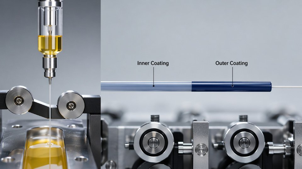
The standard fiber coating system uses two concentric acrylate layers drawn over the silica cladding immediately after the fiber exits the draw tower. The primary coating is a soft acrylate, typically running a Young’s modulus around 0.5–1.5 MPa depending on the target fiber flexibility specification; its job is to cushion the glass against lateral stress that would otherwise create microbending loss measured in fractions of a dB/km — losses that accumulate over tens of kilometers of installed cable and become commercially significant. The secondary coating is a hard acrylate, modulus in the 0.8–1.2 GPa range, providing abrasion resistance and dimensional stability during cabling operations.
Methacryloxy silanes — most commonly 3-methacryloxypropyltrimethoxysilane — and acryloxy silanes are incorporated into both layers or applied as a thin adhesion-promotion primer between the silica surface and the primary coating. The silanol groups condense with surface silanols on the silica cladding; the methacrylate group co-polymerizes into the acrylate network during UV cure. Without that covalent bridge, the primary coating strips from the cladding under repeated lateral stress cycles, a failure mode that raises attenuation in installed cables over time.
Omitting silane adhesion promotion in primary fiber coatings increases coating strip force variability by a factor of three or more, degrading process consistency and increasing post-draw rejection rates.True
Coating adhesion to silica is primarily governed by covalent siloxane bonding established by the coupling agent; purely physical adhesion is both weaker and less reproducible because it depends on surface roughness and contamination state, which vary across draw conditions.
Fiber Optic Connectors, PIC Packaging, and LIDAR Modules
Connector-grade optical adhesives and potting compounds represent a smaller volume but higher value end use. In a fiber optic connector, the adhesive bonds the fiber within a ceramic or zirconia ferrule; any delamination at the glass-adhesive interface shifts the fiber end-face geometry and increases insertion loss — even a 0.1–0.2 dB increase per connector is unacceptable in dense WDM systems where dozens of connectors appear in a single optical path. Silane-modified epoxy or acrylate adhesives — where the silane coupling agent is blended in at roughly 0.5–3% by weight, depending on the base resin and target bond strength — provide the durable glass adhesion that survives thermal shock cycling from –40°C to +85°C per IEC 61300-2-22 qualification protocols.
Photonic integrated circuit packaging and LIDAR module assembly push the same chemistry further. LIDAR lens housings and PIC chip-to-fiber coupling assemblies involve bonding glass, silicon, and polymer substrates in close proximity to active optical elements. Here the silane must not introduce fluorescence or absorption bands in the near-infrared range (850–1550 nm); formulators screen silane candidates spectrophotometrically before qualification, a step that has no equivalent in standard structural adhesive work.
UV-Curable Encapsulants for LED Arrays, CCD Sensors, and Photodetectors
Acryloxy- and methacryloxy-silanes serve a dual function in UV-curable encapsulation systems for optoelectronics: adhesion promoter and reactive diluent. As a diluent they reduce viscosity without adding a non-reactive plasticizer that would migrate over time and cloud the optical path. The critical constraint is UV transparency above 300 nm — if the silane absorbs in the same window as the photoinitiator, it competes for photons and reduces cure depth, leaving tacky under-cured zones near the substrate interface where silane concentration is highest. Qualified grades for this application carry a UV absorbance specification at 313 nm, typically below 0.05 absorbance units in a 1% solution, a spec that generic industrial-grade silanes often do not meet.
Aminosilanes are generally avoided in this segment despite their strong adhesion performance in epoxy systems, because their UV absorption profile and tendency to yellow under prolonged light exposure disqualify them for encapsulants sitting directly in the optical path of a CCD sensor or photodetector.
Silane-Functionalized Silica Nanoparticles in High-Performance Optical Coatings
Surface-treated silica nanoparticles — particle diameters typically in the 20–80 nm range, functionalized with vinylsilanes or methacryloxy silanes — are now a standard formulation tool for scratch-resistant optical coatings on camera lenses, augmented reality waveguides, and heads-up display optics. The silane surface treatment serves two purposes simultaneously: it compatibilizes the inorganic nanoparticle surface with the organic UV-curable resin matrix, preventing agglomeration that would scatter light and create haze, and it anchors the particle covalently into the cured network so that abrasion cannot pull particles free from the coating surface.
Refractive index tuning is an additional benefit. The volume fraction of silica nanoparticles, combined with the organic matrix index, allows formulators to target specific refractive indices for antireflection layer stacks without switching entirely to higher-index inorganic deposition processes. The silane surface treatment chemistry directly affects the achievable particle loading before viscosity becomes unworkable — typically 30–55% by weight in well-dispersed systems — and therefore determines how wide the refractive index tuning range actually is in practice.
Selecting the Right Silane Coupling Agent: Functional Group Compatibility and Process Parameter Guide
Choosing the wrong silane is rarely obvious at the time of formulation. The failure shows up six months later as delamination in a humidity test, adhesion loss after thermal cycling, or a PCB laminate that pulls apart at the glass-fiber interface under peel. Getting selection right means working through four filters in sequence before you ever open a sample bottle.
The Four Selection Criteria
Substrate chemistry sets the starting constraint. Silica and glass surfaces carry silanol (Si–OH) densities in the range of 2–8 hydroxyl groups per nm², depending on thermal history and surface cleaning method. Metal oxides — aluminum, copper, iron — present different reactive site densities and surface pH values, which directly affect how readily alkoxysilane hydrolysis products condense onto the surface. An aluminum oxide surface at pH 8–9 couples well with aminosilanes; the same aminosilane applied to an acidic tin-oxide surface will self-condense in solution before it ever reaches the substrate.
Polymer or resin matrix chemistry determines which organofunctional group you need on the silane’s other end. Epoxy resins react with amino and mercapto functional groups. Polyurethanes require isocyanato or amino silanes. Acrylate systems need methacryloxy or vinyl silanes for copolymerization. Polyimide — common in semiconductor dielectric and flexible circuit applications — bonds most reliably through aminosilanes forming hydrogen bonds and covalent links with the imide carbonyl. PTFE is notoriously resistant; vinyl or methacryloxy silanes with plasma pre-treatment of the PTFE surface give the best results, but do not expect the same adhesion gains you get with glass.
Process conditions are where experienced formulators earn their pay. Cure temperature matters: slower-reacting silanes like vinyltrimethoxysilane or 3-methacryloxypropyltrimethoxysilane typically need 110–150 °C to complete condensation and develop full bond strength, while aminosilanes can cure adequately at 80–100 °C. Moisture availability governs hydrolysis; in very dry environments (relative humidity below 20%), hydrolysis is incomplete and adhesion is patchy. Some production lines compensate by pre-hydrolyzing the silane in dilute aqueous solution before application.
End-use performance requirements close the selection. For high-temperature applications — think underfill materials surviving solder reflow at 260 °C — epoxy or amino silanes with short, rigid organic chain segments outperform longer-chain alternatives. Moisture resistance in high-voltage insulators or optical fiber coatings requires dense, well-crosslinked siloxane networks, which means maximizing trialkoxysilane content over dialkoxysilane.
Functional Group Compatibility Matrix
| Organofunctional Group | Compatible Resin Systems | Typical Use Concentration | Key Reaction Mechanism | Primary Electronics / Glass Application |
|---|---|---|---|---|
| Amino (–NH₂) | Epoxy, polyimide, phenolic | 0.1–0.5 wt% | Nucleophilic addition to epoxide or carbonyl | PCB laminate, semiconductor underfill, glass sizing |
| Epoxy (glycidoxy) | Epoxy, polyurethane, acrylate | 0.1–0.5 wt% | Ring-opening with amine or hydroxyl | Flip-chip encapsulant, automotive glass adhesive |
| Methacryloxy | Acrylate, unsaturated polyester | 0.1–0.3 wt% | Free-radical copolymerization | Optical fiber coating, FRP laminates |
| Vinyl | Polyethylene, polypropylene, silicone rubber | 0.05–0.2 wt% | Free-radical or peroxide crosslinking | Wire and cable, PTFE bonding |
| Mercapto (–SH) | Epoxy, polysulfide, rubber | 0.05–0.3 wt% | Thiol-ene addition, coordination to metals | Copper foil adhesion, sensor encapsulants |
| Ureido | Nylon, polyurethane, melamine | 0.1–0.4 wt% | Hydrogen bonding, carbamate formation | Glass fiber for engineering thermoplastics |
| Isocyanato | Polyurethane, epoxy | 0.1–0.3 wt% | Isocyanate-hydroxyl or amine reaction | Automotive glass sealing, polyurethane foam bonding |
Hydrolysis Rate and Pot-Life Management
Methoxysilanes hydrolyze roughly 5–10 times faster than their ethoxy counterparts under equivalent aqueous conditions.
Methoxysilanes hydrolyze 5–10× faster than ethoxysilanes under equivalent pH and temperature conditionsTrue
This rate difference is well-established in organosilane chemistry literature and stems from the lower steric hindrance and higher electrophilicity of the methoxy leaving group compared to ethoxy, accelerating nucleophilic attack by water on silicon.
That speed is an advantage for room-temperature aqueous sizing baths on glass fiber production lines, where rapid surface bonding before the fiber bundle dries is essential. The tradeoff is pot life: a freshly prepared 0.3 wt% methoxysilane bath at pH 4–5 typically has a working life of two to six hours before oligomeric condensation products accumulate and deposit unevenly on the substrate. Ethoxysilanes at similar concentrations can hold four to twelve hours, which makes them the practical choice for spray treatments on architectural glass panels or large-format laminate components where application time is extended.
Concentration: The Window Between Bare Surface and Cohesive Failure
This is the mistake most commonly seen in process scale-up. Below roughly 0.05 wt% in aqueous solution, surface coverage is incomplete — adhesion is uneven and ILSS results scatter badly across sample sets. Above 2 wt%, you are depositing multiple poorly crosslinked polysiloxane layers whose internal cohesive strength is lower than the substrate–silane bond you are trying to build. The result is a system that fails within the silane layer, not at the interface, and the failure mode looks deceptively similar to poor adhesion. Optimal coverage for most glass and silica substrates falls between 0.1 and 0.5 wt%, targeting a monolayer to bilayer regime. Actual optimum within that band depends on surface hydroxyl density, application method (dip versus spray versus size bath), and drying protocol.
Formulation Pitfalls Worth Flagging
Aminosilanes are basic — their solutions typically run pH 10–11 — and they will catalyze rapid self-condensation if added directly to an acidic aqueous formulation without adjustment. Adjust the bath to pH 4–5 first, add the silane slowly, then allow 15–30 minutes of pre-hydrolysis before introducing the substrate. Skipping this step produces gel particles in the bath within the first hour of operation.
Technical-grade silane containing pre-formed oligomers and hydrolysis byproducts is acceptable for bulk glass-fiber sizing but will undermine any application requiring monolayer control — photoresist adhesion promotion in semiconductor fabrication being the clearest example. In those contexts, semiconductor-grade or electronics-grade silane with tight specification on oligomer content and metal ion levels is not optional.
SiliconChemicals provides application-specific technical data sheets covering cure conditions, substrate preparation protocols, and compatibility data with common resin systems. REACH and RoHS compliance documentation is available for all standard product lines. Custom silane blends optimized for specific resin systems or unusual processing conditions — co-silane mixtures that balance hydrolysis rate against pot life, for instance — can be developed through a collaborative formulation program, with small qualification samples available before any volume commitment.
Quality, Purity Standards, and Supply Chain Considerations for Industrial Buyers
Purity grade is not a marketing tier — it is a reliability specification with direct consequences on yield, delamination rates, and regulatory clearance. Buying the wrong grade costs far more than the price differential on any given purchase order.
The Three-Tier Purity Landscape
Industrial grade silanes (assay 97–99% by GC) are appropriate for glass fiber sizing, construction sealants, and general rubber compounding where trace metal contamination and hydrolyzate content have no measurable effect on end-product performance. Electronic grade (assay ≥ 99.5%, residual chloride < 50 ppm, metals typically in the low-ppm range) is the correct specification for PCB laminate sizing, semiconductor packaging underfill, and molding compound formulations. Semiconductor or VLSI grade (assay ≥ 99.9%, metals < 1 ppm by ICP-MS, particle count < 10 particles/mL at 0.5 μm) is mandatory for wafer-level adhesion promotion, spin-on dielectric integration, and photolithography underlayers.
Using industrial-grade silane in a semiconductor packaging application is a cost savingFalse
Trace metal contamination from industrial-grade material introduces mobile ionic species that accelerate electromigration and corrosion in fine-pitch interconnects; the resulting reliability failures — delamination during thermal cycling, early HAST failures — generate scrap and warranty costs that dwarf any raw material savings.
The substitution risk is asymmetric: a packaging engineer running flip-chip BGA assemblies who accepts industrial grade silane to save roughly USD 2–8 per kilogram (depending on functional group and order volume) is betting the entire lot qualification against a reliability failure that may not surface until thermal cycling or moisture soak testing — weeks or months downstream.
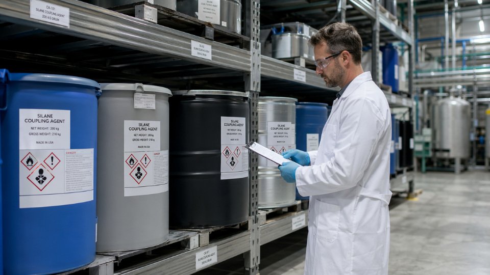
Certificate of Analysis: What to Actually Demand
A CoA from a credible supplier should include, at minimum: GC assay (%), water content by Karl Fischer titration (< 200 ppm for electronic grade; < 100 ppm is achievable and preferable), APHA color (< 20 for electronics applications), refractive index at 20°C, density at 20°C, and residual chloride content (< 50 ppm electronic grade; < 5 ppm semiconductor grade). For semiconductor and VLSI grade material, insist on a full ICP-MS trace metals panel covering Na, K, Fe, Ca, Al, Cu, Cr, Ni, Zn, and Pb at minimum. Any supplier unable to provide lot-specific ICP-MS data for high-purity grades should not be on your approved vendor list for front-end fab applications.
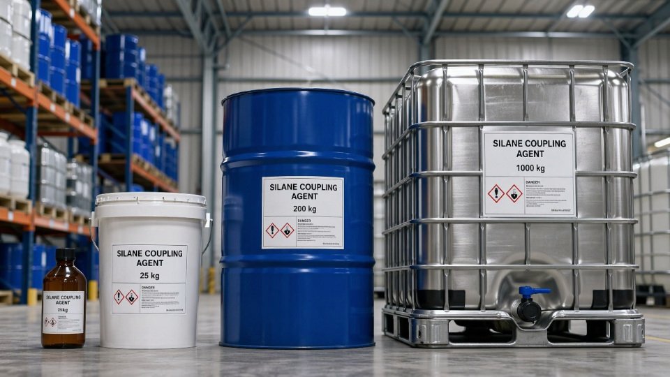
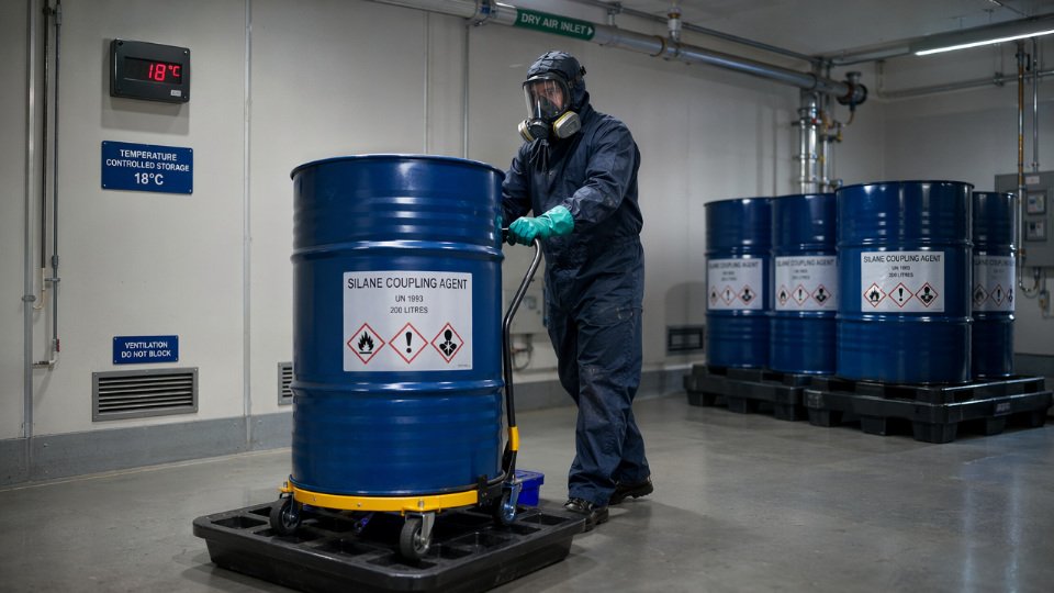
Packaging, Storage, and Shelf Life
Silanes hydrolyze in the presence of moisture — some functional groups faster than others, but all are susceptible. Correct packaging means dry nitrogen or argon blanket in sealed moisture-barrier containers: stainless steel drums for bulk quantities, HDPE bottles with foil-lined closures for smaller volumes. Storage temperature should be maintained between 5°C and 25°C, away from direct sunlight and humidity excursions. Shelf life under correct storage is typically 12–24 months depending on functional group reactivity; chloroalkylsilanes and aminosilanes sit on opposite ends of that range. Material that has been moisture-contaminated during transit or warehouse storage degrades to hydrolyzed oligomers that will not form the intended monolayer on the substrate surface — you get inconsistent adhesion and no obvious incoming inspection failure until process yield drops.
Specify incoming Karl Fischer testing as a receiving inspection step. It takes under 30 minutes and catches contaminated lots before they reach your coating line.
Regulatory Compliance in Global Electronics Supply Chains
Electronics manufacturers supplying European, North American, and Japanese OEMs face a layered compliance burden. Require REACH SVHC declaration (current candidate list), RoHS 3 (EU Directive 2015/863) confirmation that the silane treatment process introduces no restricted substances into the finished assembly, and TSCA inventory status for US imports. For China-manufactured or China-destined product, confirm alignment with applicable GB standards for hazardous substance control. Reputable suppliers provide these declarations proactively with each shipment — not only on request. Chasing compliance documentation reactively during a customer audit is an avoidable operational problem.
Supply Chain Geography and Resilience
China’s Zhejiang, Jiangsu, and Shandong provinces collectively host the world’s largest integrated organosilicon production clusters. The proximity of trichlorosilane and methylchlorosilane intermediate production to silane coupling agent synthesis in these regions compresses raw material lead times, reduces intermediate handling steps, and creates energy and logistics cost structures that European and North American standalone silane producers cannot easily replicate. SiliconChemicals operates within this cluster, with finished goods moving through Shanghai and Ningbo ports — both offering consistent freight connectivity to Southeast Asia, Europe, and the Americas. Lot-to-lot consistency is a direct beneficiary of this integration: when the same intermediate streams feed the same reactors under stable process control, batch variability narrows.
Qualifying a New Silane Supplier
Qualification for electronics-grade applications is not a one-shipment evaluation. A realistic protocol runs incoming QC testing on the first three lots (GC assay, Karl Fischer, chloride, ICP-MS where applicable), followed by process qualification runs on representative substrates, followed by accelerated reliability testing — typically 1,000 hours HAST or 500 thermal cycles depending on the application. Document adhesion strength, delamination incidence, and ionic contamination before changing approved vendor status. Audit rights matter: the ability to conduct an on-site factory visit or commission a third-party audit of manufacturing process documentation, raw material traceability, and quality management records is a legitimate expectation for any supplier entering an electronics bill of materials. SiliconChemicals supports third-party audits and provides full process transparency — batch records, raw material certificates, and in-process control data — because buyers in this industry have every right to verify what they cannot see from a CoA alone.
Emerging Applications: Silane Coupling Agents in Advanced Packaging, Flexible Electronics, and Photovoltaics
The electronics industry rarely stands still long enough for a single chemistry to become obsolete. Silane coupling agents are proving this out: architectures that didn’t exist commercially five years ago are now creating entirely new bonding challenges, and silane chemistry is at the center of most solutions.
Advanced Semiconductor Packaging: FOWLP, Chiplets, and Heterogeneous Integration
Fan-out wafer-level packaging (FOWLP) and chiplet-based heterogeneous integration have multiplied the number of dissimilar material interfaces inside a single package. The redistribution layer (RDL) alone may stack polyimide or polybenzoxazole (PBO) dielectrics against copper metallization, silicon oxide, and silicon nitride — each with different surface energy and thermal expansion. Without controlled adhesion promotion at each interface, delamination initiates during the thermal cycling that qualification tests demand.
Benzocyclobutene (BCB)-functional silanes and PBO-compatible aminosilane primers are in active development specifically to address RDL dielectric adhesion in FOWLP and 3D-IC packages.True
Multiple materials suppliers and academic groups working on advanced packaging dielectrics have published work on functionalized silane primers for low-temperature curable polymer dielectrics; this is well-documented in IEEE ECTC and IMAPS conference proceedings from 2020 onward.
Through-silicon via (TSV) sidewall passivation is another area where silane treatment earns its place. The SiO₂ or Si₃N₄ liner deposited inside a TSV is a narrow, high-aspect-ratio surface that must bond reliably to the polymer fill or copper barrier. Even a 10–20 nm silane coupling layer applied by vapor-phase treatment meaningfully reduces interfacial void formation. The processing window is tight — temperature, exposure time, and moisture content all interact — but the consequence of skipping it shows up as leakage or mechanical failure in reliability testing, not during fabrication.
Flexible and Printed Electronics: The Low –OH Problem
Glass has abundant surface hydroxyl groups. Polyimide, PET, and PEN do not. On a typical polyimide film, –OH site density can be two to three orders of magnitude lower than on borosilicate glass, which means the standard silane treatment process used for glass fiber or silicon wafers simply doesn’t generate enough covalent bonds to hold an ITO or IGZO thin film through bending cycles.
The practical fix is a pre-activation step — UV-ozone treatment for 3–10 minutes or O₂ plasma for 30–120 seconds — before silane application. This generates the carbonyl and hydroxyl surface groups that give the silane something to react with. Skip the activation and silane contact angle measurements may look acceptable while adhesion in a peel test fails badly. The activation window matters too: activated polyimide surfaces can rehydroxylate or oxidize further within hours in ambient air, so the process sequence from activation through silane application and film deposition needs to be tightly scheduled.
Photovoltaics: Perovskite Passivation and Silicon Module Encapsulants
In silicon PV module manufacturing, silane-based adhesion promoters in EVA and POE encapsulant formulations are standard. The silane ties the encapsulant polymer to glass and backsheet surfaces, keeping peel strength above acceptable thresholds through 25-year outdoor exposure cycles. Aminosilane concentrations in encapsulant formulations typically run 0.1–0.5 wt%, with the optimum depending on EVA grade and lamination temperature.
Perovskite PV is a different challenge. Undercoordinated Pb²⁺ defects at grain boundaries act as recombination centers that suppress voltage and fill factor. Aminosilanes and thiosilanes — the thiol or amine group coordinates to Pb²⁺ directly — have shown 0.5–1.5 percentage points of absolute power conversion efficiency improvement in published cell studies, depending on perovskite composition, defect density, and treatment concentration. This isn’t a volume market yet, but the quantities demanded per GW of capacity are small enough that high-purity specialty silanes command pricing well above commodity grades.
Quantum Dot and Mini-LED Displays
Quantum dot films and color conversion layers are moisture-sensitive. Silane surface treatment of the QD encapsulant matrix — typically a silicone or acrylate — and of the inorganic filler particles within it improves barrier properties and slows oxygen and water ingress at film edges and interfaces. Under accelerated aging (85°C/85% RH), treated formulations have demonstrated lifetime extensions from the hundreds-of-hours range into the low thousands, a gap that matters when display manufacturers are quoting 50,000-hour panel lifetimes.
High-Loading EMC and Underfill for Thermal Management
As the power density of advanced chips rises, molding compounds and underfills are being reformulated with filler loadings above 90 wt% silica or aluminum nitride — levels that create severe rheology problems if filler surfaces aren’t treated. Silane coupling agent treatment of the filler, applied either during filler manufacturing or in a dry-blend step before compounding, reduces agglomeration and lowers melt viscosity enough to allow complete mold fill in fine-pitch packages. The silane functional group must be matched to the resin system: epoxy-functional silanes for epoxy-novolac EMC, methacrylate-functional silanes where compatibility with the crosslink chemistry demands it. Getting this wrong at 90+ wt% loading shows up immediately as short shots, voids, or wire sweep — not as a subtle reliability issue discovered later.
Frequently Asked Questions About Silane Coupling Agents in Electronics and Glass
What is the difference between a silane coupling agent and a silane adhesion promoter?
The two terms get used interchangeably in most technical datasheets, but the distinction matters when you are specifying materials for a qualification protocol. A silane coupling agent is specifically bifunctional — one end bonds covalently to an inorganic surface (glass, silica, metal oxide), the other reacts chemically with the organic polymer matrix. That dual-bond architecture is the defining feature. “Adhesion promoter” is a broader category: it includes silanes applied as thin surface primers where the primary function is surface energy modification or mechanical interlocking rather than a through-bond molecular bridge. Every silane coupling agent can serve as an adhesion promoter, but a silane-based primer formulated to improve wetting on a painted substrate may not form the bifunctional covalent bridge that defines a true coupling agent. When your process spec calls for “adhesion promoter,” verify whether bifunctional bonding is actually required — the answer changes which chemistry and which concentration you need.
Can silane coupling agents improve adhesion on aluminum and copper, not just glass?
Yes, and this is under-appreciated outside the PCB and aerospace adhesive communities. Both aluminum oxide (Al₂O₃) and the mixed copper oxides (CuO and Cu₂O) that naturally form on copper surfaces carry surface hydroxyl groups. Hydrolyzed silanes react with these hydroxyls to form Si–O–Al and Si–O–Cu bonds that are thermally stable up to roughly 200–300 °C depending on oxide stoichiometry and silane type. Aminosilanes and epoxysilanes are the workhorses here — aminosilanes for copper foil in PCB laminates and for aluminum bonding in structural aerospace assemblies, epoxysilanes where the resin system is epoxy-based and functional-group matching is straightforward.
Effectiveness depends heavily on two factors: oxide layer thickness and surface cleanliness. A thick, uncontrolled oxide on aluminum reduces silane bond density. Copper that has oxidized unevenly after etching gives inconsistent adhesion. Pre-treatment — either acid micro-etch or plasma clean — is usually necessary before silane application to get reproducible bond strength.
Hydrolyzed aminosilanes and epoxysilanes form stable covalent bonds with aluminum oxide and copper oxide surface hydroxyls, enabling use on metal substrates beyond glass and silica.True
Surface hydroxyl groups on Al₂O₃, CuO, and Cu₂O are chemically equivalent reaction sites for hydrolyzed alkoxysilanes; Si–O–metal bonds formed via condensation are well-documented in the adhesion science literature and confirmed by XPS surface analysis in published PCB and aerospace adhesive studies.
How do you apply a silane coupling agent — concentration, solvent, and process parameters?
For aqueous systems, dissolve the silane at 0.1–2.0 wt% in deionized water, adjust pH to 4–5 with acetic acid (critical for methoxysilanes — alkaline conditions accelerate self-condensation before the silane reaches the substrate), and allow 30–60 minutes of hydrolysis time before application. Apply by spray, dip, or wipe, then cure at 80–120 °C for 5–15 minutes. Where water compatibility is a concern, use 0.5–2.0 wt% in isopropanol/water (95:5 by volume) — this slows hydrolysis enough to extend bath life while still delivering sufficient silanol groups for surface reaction. Air-dry is acceptable for solvent systems, though a brief thermal step improves condensation completeness.
Those ranges are starting points. The right concentration for a glass-fiber sizing operation running at line speed is different from a batch dip process for optical components. Validate each combination of substrate, silane type, and resin system in your own process — don’t carry parameters over from a different application without testing.
What shelf life should I expect, and how should silanes be stored?
Properly sealed, moisture-free silanes stored at 15–25 °C under inert gas typically remain within specification for 12–24 months. Aminosilanes sit at the short end of that range — they are more reactive toward hydrolysis and self-condensation, and 12 months from manufacture is a practical working limit. Chlorosilane-derived products are even more sensitive.
Once a container is opened, reseal it immediately under dry nitrogen. Never return used or partially hydrolyzed silane to the original container — you risk contaminating the entire drum, which in a high-volume electronics process means failed adhesion across potentially thousands of assemblies before the cause is traced back to the raw material. In practice, size your orders to match consumption within one production cycle rather than buying for minimum unit price and holding inventory too long.
What safety precautions apply during handling?
Most commercial silane coupling agents — aminosilanes, epoxysilanes, methacryloxy silanes — are classified as irritants. Nitrile gloves, safety glasses, and local exhaust ventilation are the baseline. The specific hazard that catches operations teams off guard is methanol release during hydrolysis of methoxysilanes. Methanol is toxic by both inhalation and skin absorption, and the quantities released in a heated dip tank or spray booth accumulate faster than people expect. A dedicated ventilation calculation for your process volume is not optional.
Chlorosilane intermediates are corrosive and moisture-reactive; these should be handled only in dedicated equipment by trained personnel. Finished coupling agent formulations are generally not classified as dangerous goods under ADR, IMDG, or IATA for standard shipping, but moisture-proof packaging and clear labeling remain mandatory.
How does SiliconChemicals maintain lot-to-lot consistency for volume electronics manufacturing?
Lot-to-lot variation is the practical failure mode that procurement managers rarely ask about until it causes a process excursion. SiliconChemicals operates ISO 9001-certified production with in-process gas chromatography monitoring at multiple synthesis stages, dedicated electronic-grade production lines to eliminate cross-contamination from industrial-grade products, and 100% lot release testing against full specification before any shipment leaves the facility. Every shipment includes a complete Certificate of Analysis, batch-specific analytical data, and retained reference samples held for a defined period should any field issue require investigation.
For customers running formally qualified processes — which describes most semiconductor packaging and PCB laminate operations — long-term supply agreements include a guaranteed specification freeze period. That means SiliconChemicals cannot change raw material sourcing, synthesis route, or specification limits within that window without advance notification and a defined transition protocol. Process requalification triggered by a supplier’s unannounced raw material change is expensive and time-consuming; the freeze commitment is there specifically to prevent it.